Etude et réalisation d'un émetteur à infrarouge( Télécharger le fichier original )par Randa et Lamia BEDRA et BARKAT Université de Batna Algérie - Licence en électronique 2011 |

~onc(usion genera(Notre projet vise à réaliser un émetteur infrarouge. Ce travail nous a permis, premièrement, d'approfondir nos connaissances théoriques en cherchant dans différentes sources de documentation, les composants nécessaires et les techniques adéquates qui peuvent nous aider à résoudre certains problèmes. Ensuite, l'application de ces connaissances dans la pratique nous a permis d'apprendre à manipuler ces composants de façon plus concrète. Tous ces efforts, ont donc donné naissance à ce modeste, que nous considérons comme le fruit d'une première expérience très intéressante sur tous les plans. Cette réalisation serait, néanmoins amélioré par un récepteur infrarouge ( pour ondes moyennes par exemple), qui permettrait de recevoir des émetteurs locaux ou étrangers( la nuit) ou être utilisé dans des système antivol.
Liste ties Composants
| |||||||||||||||||||||||||||||||||||||||||||||||||||||||||||||||||||||||||||||||||||||||||||||||||||||||||||||||||||||||||||||||||||||||||||||||||||||||||||||||||||||||||||||||||||||||||||||||||||||||||||||||||||||||||||||||||||||||||||||||||||||||||||||||||||||||||||||||||||||||||||||||||||||||||||||||||||||||||||||||||||||||||||||||||||||||||||||||||||||||||||||||||||||||||||||||||||||||||||||||||||||||||||||||||||||||||||||||||||||||||||||||||||||||||||||||||||||||||||||||||||||||||||||||||||||||||||||||||||||||||||||||||||||||||||||||||||||||||||||||||||||||||||||||||||||||||||||||||||||||||||||||||||||||||||||||||||||||||||||||||||||||||||||||||||||||||||||||||||||||||||||||||||||||||||||||||||||||||||||||||||||||||||||||||||||||||||||||||||||||||||||||||||||||||||||||||||||||||||||||||||||||||||||||||||||||||||||||||||||||||||||||||||||||||||||||||||||||||||||||||||||||||||||||||||||||||||||||||||||||||||||||||||||||||||||||||||||||||||||||||||||||||||||||||||||||||||||||||||||||
|
DESCRIPTION |
TEMPERATURE RANGE |
ORDER CODE |
DWG # |
|
8-Pin Plastic Small Outline (SO) Package |
0 to +70°C |
NE555D |
0174C |
|
8-Pin Plastic Dual In-Line Package (DIP) |
0 to +70°C |
NE555N |
0404B |
|
8-Pin Plastic Dual In-Line Package (DIP) |
-40°C to +85°C |
SA555N |
0404B |
|
8-Pin Plastic Small Outline (SO) Package |
-40°C to +85°C |
SA555D |
0174C |
|
8-Pin Hermetic Ceramic Dual In-Line Package (CERDIP) |
-55°C to +125°C |
SE555CFE |
|
|
8-Pin Plastic Dual In-Line Package (DIP) |
-55°C to +125°C |
SE555CN |
0404B |
|
14-Pin Plastic Dual In-Line Package (DIP) |
-55°C to +125°C |
SE555N |
0405B |
|
8-Pin Hermetic Cerdip |
-55°C to +125°C |
SE555FE |
|
|
14-Pin Ceramic Dual In-Line Package (CERDIP) |
0 to +70°C |
NE555F |
0581B |
|
14-Pin Ceramic Dual In-Line Package (CERDIP) |
-55°C to +125°C |
SE555F |
0581B |
|
14-Pin Ceramic Dual In-Line Package (CERDIP) |
-55°C to +125°C |
SE555CF |
0581B |
Timer NE/SA/SE555/SE555C
BLOCK DIAGRAM
VCC
8
·
THRESH-
OLD
6 0--
COMPARATOR
CONTROL
VOLTAGE
0 5
TRIGGER --0 2
DIS-
CHARGE
7 0
FLIP FLOP
RESET
0 4
COMPARATOR
OUTPUT
STAGE
0 3 O 1
OUTPUT GND
EQUIVALENT SCHEMATIC
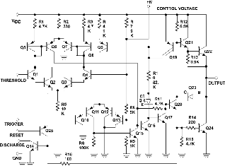
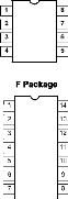
NOTE: Pin numbers are for 8-Pin package
Timer NE/SA/SE555/SE555C
ABSOLUTE MAXIMUM RATINGS
|
SYMBOL |
PARAMETER |
RATING |
UNIT |
|
Supply voltage |
|||
|
Vcc |
SE555 |
+18 |
V |
|
NE555, SE555C, SA555 |
+16 |
V |
|
|
PD |
Maximum allowable power dissipation1 |
600 |
mW |
|
TA |
Operating ambient temperature range |
||
|
NE555 |
0 to +70 |
°C |
|
|
SA555 |
-40 to +85 |
°C |
|
|
SE555, SE555C |
-55 to +125 |
°C |
|
|
TSTG |
Storage temperature range |
-65 to +150 |
°C |
|
TSOLD |
Lead soldering temperature (10sec max) |
+300 |
°C |
NOTES:
1. The junction temperature must be kept below 125°C for the D package and below 150°C for the FE, N and F packages. At ambient temperatures above 25°C, where this limit would be derated by the following factors:
D package 160°C/W FE package 150°C/VV N package 100°C/W F package 105°C/W
Timer NE/SA/SE555/SE555C
DC AND AC ELECTRICAL CHARACTERISTICS
TA = 25°C, Vcc = +5V to +15 unless otherwise specified.
|
SE555 |
NE555/SE555C |
||||||||
|
SYMBOL |
PARAMETER |
TEST CONDITIONS |
UNIT |
||||||
|
Min |
Typ |
Max |
Min |
Typ |
Max |
||||
|
Vcc |
Supply voltage |
4.5 |
18 |
4.5 |
16 |
V |
|||
|
ICC |
Supply current (low |
Vcc=5V, RL=0. |
3 |
5 |
3 |
6 |
mA |
||
|
state)1 |
Vcc=15V, RL=oo |
10 |
12 |
10 |
15 |
mA |
|||
|
Timing error (monostable) |
RA=2k52 to 1001d2 |
||||||||
|
tM |
Initial accuracy2 |
C=0.1gF |
0.5 |
2.0 |
1.0 |
3.0 |
% |
||
|
Atm/AT |
Drift with temperature |
30 |
100 |
50 |
150 |
ppm/°C |
|||
|
AtM/AVS |
Drift with supply voltage |
0.05 |
0.2 |
0.1 |
0.5 |
%N |
|||
|
Timing error (astable) |
RA, Rs=1k52 to 100kO |
||||||||
|
to |
Initial accuracy2 |
C=0.1gF |
4 |
6 |
5 |
13 |
% |
||
|
AtA/AT |
Drift with temperature |
Vcc=15V |
500 |
500 |
ppm/°C |
||||
|
AtA/AVS |
Drift with supply voltage |
0.15 |
0.6 |
0.3 |
1 |
%N |
|||
|
VC |
Control voltage level |
Vcc=15V |
9.6 |
10.0 |
10.4 |
9.0 |
10.0 |
11.0 |
V |
|
Vcc=5V |
2.9 |
3.33 |
3.8 |
2.6 |
3.33 |
4.0 |
V |
||
|
VTH |
Threshold voltage |
Vcc=15V |
9.4 |
10.0 |
10.6 |
8.8 |
10.0 |
11.2 |
V |
|
ITH |
Threshold current3 |
Vcc=5V |
2.7 |
3.33 |
4.0 |
2.4 |
3.33 |
4.2 |
V |
|
VTRIG |
Trigger voltage |
Vcc=15V |
4.8 |
5.0 |
5.2 |
4.5 |
5.0 |
5.6 |
V |
|
'TRIG VRESET |
Trigger current |
Vcc=5V |
1.45 |
1.67 |
1.9 |
1.1 |
1.67 |
2.2 |
V V |
|
'RESET |
Reset current |
VREsET=0.4V |
0.1 |
0.4 |
0.1 |
0.4 |
mA |
||
|
Reset current |
VREsET=OV |
0.4 |
1.0 |
0.4 |
1.5 |
mA |
|||
|
Vcc=15V |
|||||||||
|
IsiNk=10mA |
0.1 |
0.15 |
0.1 |
0.25 |
V |
||||
|
Vol |
Output voltage (low) |
IsiNk=50mA |
0.4 |
0.5 |
0.4 |
0.75 |
V V |
||
|
lsiNk=200mA |
2.5 |
V |
2.5 |
||||||
|
VCC=5V |
|||||||||
|
IsiNk=8mA |
0.1 |
0.25 |
0.3 |
0.4 |
V |
||||
|
IsiNk=5mA |
0.05 |
0.2 |
0.25 |
0.35 |
V |
||||
|
Vcc=15V |
|||||||||
|
ISOURCE=200MA |
12.5 |
V |
12.5 |
||||||
|
VOH |
Output voltage (high) |
'SOURCE= 1 00mA |
13.0 |
13.3 |
12.75 |
13.3 |
V |
||
|
VCC=5V |
|||||||||
|
tOFF |
Turn-off times |
IsouRcE=100mA VRESET=VCC |
3.0 |
3.3 |
2.0 |
2.75 |
3.3 |
2.0 |
V |
|
tR |
Rise time of output |
100 |
200 |
100 |
300 |
ns |
|||
|
tF |
Fall time of output |
100 |
200 |
100 |
300 |
ns |
|||
|
Discharge leakage current |
20 |
100 |
20 |
100 |
nA |
||||
NOTES:
1. Supply current when output high typically lmA less.
2. Tested at Vcc=5V and Vcc=15V.
3. This will determine the max value of RA+RB, for 15V operation, the max total R=10MO, and for 5V operation, the max. total R=3.4MO.
4. Specified with trigger input high.
5. Time measured from a positive going input pulse from 0 to 0.8xVcc into the threshold to the drop from high to low of the output. Trigger is tied to threshold.
Timer NE/SA/SE555/SE555C
0 0 1 0.2 0 3 0.4 (XVCC)
LOWEST VOLTAGE LEVEL OF TRIGGER PULSE
SUPPLY VOLTAGE - VOLTS
5.0 10.0 15.0
-50 -25 0 +25 +50 +75 +100+125
TEMPERATURE - °C
10
1.0
VOUT --VOLTS
0.1
100
100
1 0 2.0
1 0 2.0
50 100
5.0 10 20 50
5.0 10 20 50
(SINK - mA
(SINK mA
(SINK mA
Delay Time
vs Supply Voltage
High Output Voltage Drop
vs Output Source
Current
Propagation Delay vs Voltage
Level of Trigger
Pulse
20
1.0
20
50 100
5 0 10 20
'SOURCE - mA
0 5 10 15
SUPPLY VOLTAGE - V
0 01 02 03 04
LOWEST VOLTAGE LEVEL
OF TRIGGER PULSE - XVcc
Low Output Voltage
vs Output Sink
Current
Low Output Voltage
vs Output Sink
Current
Low Output Voltage
vs Output Sink
Current
|
I I I Vcc = 10V _ |
||||||
|
-55°C |
ApP.--- M |
|||||
|
+25°C |
||||||
|
1+25°C |
||||||
|
+25°C MP" |
||||||
|
+25°C .7): 17:2- |
||||||
|
---'''- |
||||||
I I I
0.01
10
10
1.015
1.010
0.985
V CC VOUT -- VOLTS
2.0
1.8
1.6
1.4
1.2
1.0
0.8
0.6
0.4 0.2 0
+125°C
-55°C
+25°C
5V Vcc 15V
NORMALIZED DELAY TIME
300
1.005
0.995
0.990
1.000
PROPAGATION DELAY -- ns
250
200
150
100
50
+25°C
SUPPLY CURRENT -- mA
8.0
6.0
4.0
2.0
Minimum Pulse Width
Required for
Triggering
Supply Current Delay Time
vs Supply Voltage vs Temperature
1.015
·
·
·
·
·
·
150
7, 125
8 100
w
w
01 75
2 50
7
2 z
25
10.0
NORMALIZED DELAY TIME
0
1.010
1.005
1.000
0.995
0.990
0.985
10
1.0
to
0
1- 0.1
7
0
0.01
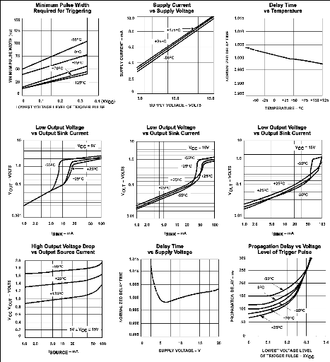
TYPICAL PERFORMANCE CHARACTERISTICS
Timer NE/SA/SE555/SE555C
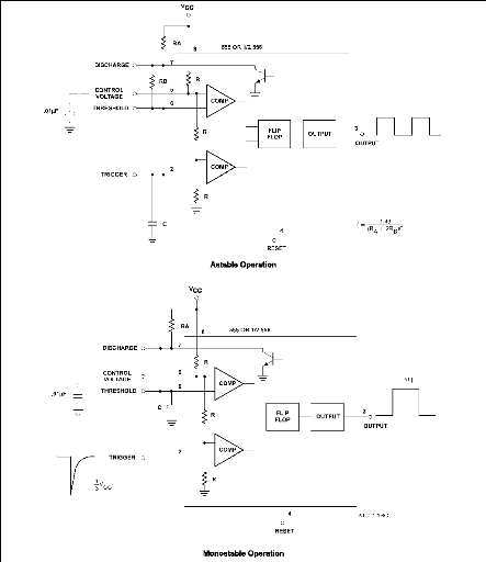
CONTROL - VOLTAGE
.01pF THRESHOLD
DISCHARGE
7-7
TRIGGER
vcc
Astable Operation
vcc
DISCHARGE
CONTROL
VOLTAGE
.01pF 1 THRESHOLD
1:
3V
TRIGGER
Monostable Operation
TYPICAL APPLICATIONS
Timer NE/SA/SE555/SE555C
TYPICAL APPLICATIONS
NOTE: All resistor values are in Q
Figure 1. AC Coupling of the Trigger Pulse
Trigger Pulse Width Requirements and Time Delays
Due to the nature of the trigger circuitry, the timer will trigger on the negative going edge of the input pulse. For the device to time out properly, it is necessary that the trigger voltage level be returned to some voltage greater than one third of the supply before the time out period. This can be achieved by making either the trigger pulse sufficiently short or by AC coupling into the trigger. By AC coupling the trigger, see Figure 1, a short negative going pulse is achieved when the trigger signal goes to ground. AC coupling is most frequently used in conjunction with a switch or a signal that goes to ground which initiates the timing cycle. Should the trigger be held low, without AC coupling, for a longer duration than the timing cycle the output will remain in a high state for the duration of the low trigger signal, without regard to the threshold comparator state. This is due to the predominance of Q15 on the base of Q16, controlling the state of the bi-stable flip-flop. When the trigger signal then returns to a high level, the output will fall immediately. Thus, the output signal will follow the trigger signal in this case.
Another consideration is the 'turn-off time". This is the measurement of the amount of time required after the threshold reaches 2/3 Vcc to turn the output low. To explain further, Q1 at the threshold input turns on after reaching 2/3 Vcc, which then turns on Q5, which turns on Q6. Current from Q6 turns on Q16 which turns Q17 off. This allows current from Q19 to turn on Q20 and Q24 to given an output low. These steps cause the 2jts max. delay as stated in the data sheet.
Also, a delay comparable to the turn-off time is the trigger release time. When the trigger is low, Qic, is on and turns on Q11 which turns on Q15. Q15 turns off Q16 and allows Q17 to turn on. This turns off current to Q20 and Q24, which results in output high. When the trigger is released, Q10 and Q11 shut off, Q15 turns off, Q16 turns on and the circuit then follows the same path and time delay explained as "turn off time". This trigger release time is very important in designing the trigger pulse width so as not to interfere with the output signal as explained previously.
SIEMENS
GaAs-IR-Lumineszenzdiode GaAs Infrared Emitter
Area not flat
0.6
0.4
OQ
C)
I
5.9
5.5
0.6
0.4
E
E .5
c=,_
1.8
1.2
29
27
Cathode (Diode) Collector (Transistor) Approx. weight 0.5 g
00.
Chip position
2
9.0
8.2
7.8
7.5
GEX06260
5.7
5.1 -6--
0 CO CNI CO 0 X CD
Malle in mm, wenn nicht anders angegeben/Dimensions in mm, unless otherwise specified.
Wesentliche Merkmale
· Sehr enger Abstrahlwinkel
· GaAs-IR-LED, hergestellt im
Schmelzepitaxieverfahren· Hohe Zuverlassigkeit
· Hohe Impulsbelastbarkeit
· Gruppiert lieferbar
· Gehausegleich mit SFH 484
Anwendungen
· IR-Fernsteuerung von Fernseh- and Rundfunkgeraten, Videorecordern, Lichtdimmern, Gersten
Features
· Extremely narrow half angle
· GaAs infrared emitting diode, fabricated in a liquid phase epitaxy process
· High reliability
· High pulse handling capability
· Available in groups
· Same package as SFH 484
Applications
· IR remote control of hi-fi and TV-sets, video tape recorders, dimmers,
of various equipment
|
Typ Type |
Bestellnummer Ordering Code |
Gehause |
|
LD 274 |
Q62703-Q1031 |
5-mm-LED-Gehause (T 1 3/4), graugettintes EpoxyGiel,harz, Anschlusse im 2.54-mm-Raster (1/101 Kathodenkennzeichnung: Kurzerer Lotspiefl, flat 5 mm LED package (T 1 3/4), grey colored epoxy resin lens, solder tabs lead spacing 2.54 mm (1/10"), cathode marking: shorter solder lead, flat |
|
LD 274-21) |
Q62703-Q1819 |
|
|
LD 274-3 |
Q62703-Q1820 |
1) Nur auf Anfrage lieferbar. 1) Available only on request.
Grenzwerte (TA = 25 °C) Maximum Ratings
|
Bezeichnung Description |
Symbol |
Wert Value |
Einheit Unit |
|
Betriebs- und Lagertemperatur Operating and storage temperature range |
T op T 1 stg |
-- 55 ... + 100 |
°C |
|
Sperrschichttemperatur Junction temperature |
T , |
100 |
°C |
|
Sperrspannung Reverse voltage |
VR |
5 |
V |
|
Durchlaastrom Forward current |
IF |
100 |
mA |
|
Stollstrom, tp = 10us, D = 0 Surge current |
-IFSM |
3 |
A |
|
Verlustleistung Power dissipation |
Ptot |
165 |
mW |
|
Warmewiderstand Thermal resistance |
RthJA |
450 |
K/W |
Kennwerte (TA = 25 °C) Characteristics
|
Bezeichnung Description |
Symbol |
Wert Value |
Einheit Unit |
|
Wellenlange der Strahlung Wavelength at peak emission IF = 100 mA, tp = 20 ms |
kpeak |
950 |
nm |
|
Spektrale Bandbreite bei 50 % von Imax Spectral bandwidth at 50 % of Imax /F = 100 m A, tp = 20 ms |
AX |
55 |
nm |
|
Abstrahlwinkel Half angle |
ce |
#177; 10 |
Grad |
|
Aktive Chipflache Active chip area |
A |
0.09 |
mm2 |
|
Abmessungen der aktive Chipflache Dimension of the active chip area |
L x B L x W |
0.3 x 0.3 |
mm |
|
Abstand Chipoberflache bis Linsenscheitel Distance chip front to lens top |
H |
4.9 ... 5.5 |
mm |
|
Schaltzeiten, Ie von 10 % auf 90 % und von 90 % auf 10 %, bei IF = 100 mA, RL = 50 SI Switching times, I. from 10 % to 90 % and from 90 % to 10 %, IF = 100 mA, RL = 50 SI |
tr, tf |
1 |
Rs |
Kennwerte (TA = 25 °C) Characteristics
|
Bezeichnung Description |
Symbol |
Wert Value |
Einheit Unit |
|
Kapazitat Capacitance VR = 0 V, f = 1 MHz |
Ce |
25 |
pF |
|
Durchlallspannung Forward voltage IF = 100 mA, tp = 20 ms IF = 1 A, tp = 100 .ts |
VF |
1.30 1.5) 1.90 2.5) |
V |
|
Sperrstrom, VR = 5 V Reverse current |
IR |
0.01 1) |
RA |
|
Gesamtstrahlungsflufl Total radiant flux IF = 100 mA, tp = 20 ms |
(De |
15 |
mW |
|
Temperaturkoeffizient von Ie bzw. (I)e, IF = 100 mA Temperature coefficient of 1. or (De, IF = 100 mA |
TC, |
-- 0.55 |
%X |
|
Temperaturkoeffizient von VF, IF = 100
mA |
TCv |
-- 1.5 |
mV/K |
|
Temperaturkoeffizient von X, IF = 100 mA Temperature coefficient of X, IF = 100 mA |
TCA, |
+ 0.3 |
nm/K |
Gruppierung der Strahlstarke I. in Achsrichtung gemessen bei einem Raumwinkel S2 = 0.001 sr Grouping of radiant intensity le in axial direction at a solid angle of SI = 0.001 sr
|
Bezeichnung Description |
Symbol |
Wert |
Einheit Unit |
||
|
LD 274 |
LD 274-21) |
LD 274-3 |
|||
|
Strahlstarke |
Ie min |
50 |
50 |
80 |
mW/sr |
|
Radiant intensity |
Ie max |
-- |
100 |
-- |
mW/sr |
|
IF = 100 mA, tp = 20 ms |
|||||
|
Strahlstarke |
|||||
|
Radiant intensity |
|||||
|
IF = 1 A, tp = 100 45 |
le tYP. |
350 |
600 |
800 |
mW/sr |
1) Nur auf Anfrage lieferbar. 1) Available only on request.
SIEMENS
|
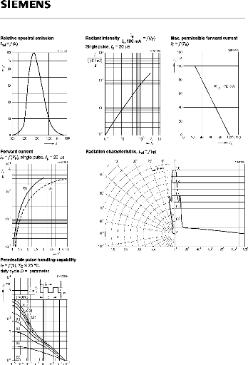
Relative Irel=f 100 Irel 80 60 40 20 0 |
spectral emission (X) OH 001938 |
Radiant intensity Single pulse, 102 |
tp = |
f |
(IF) OHR01038 |
IF =f (TA) F mA 100 80 60 40 20 0 |
Max. permissible forward current 0HR00883 |
|||||||||||||||||||
|
Ie 100 mA 20 j.ts |
||||||||||||||||||||||||||
|
Ie (100 |
mA) 101 10° 10 10 |
|||||||||||||||||||||||||
|
RthjA |
450 |
K/W |
||||||||||||||||||||||||
|
880 920 960 |
1000 |
nm 1060 A |
10 1 |
0° A |
101 |
0 20 40 60 80 100 °C 120 TA |
||||||||||||||||||||
|
CIF |
||||||||||||||||||||||||||
Forward current
IF = f (VF), single pulse tp = 20 las
10 1 0HR01041
IF A
10°
10-1
102
15 2 25 3 35 4 V 4 5
VF
Permissible pulse handling capability IF =f (t), Tc < 25 °C,
duty cycle D = parameter
104
IF mA
5
5
102
10-5 101 10-3 10-2 101 10° 101 8102
0HR00860
max.
YP.
1
Radiation characteristics, Ire! =f ((p)
40°
0°
10°
1.0
0.8
0.6
0.4
20°
40°
60°
80°
100° 120°
50°
Emu Emu NNE;
Non Non Nom
IIIIIIII
111111 1/111/11
D = 0 005
I
161E1111111111111111111
PI nil 0 02
hi& 0 05
II.kIL MEM MEM MEM NMI EM
111:41 Man
NM
·
·Il 111
·
·Il
·
·Il
·
·Il
·
·
111 %V111
·111111
0.2
Mk MI
MI11111111111
1111111111115al 1111111111 111111
1111 111 1:1 11
11111111111110
IN