CONCLUSION GÉNÉRALE
Dans le cadre de notre travail, nous avons
étudié les interrupteurs à semi-conducteurs de puissance,
ensuite nous avons étudié quelques types des convertisseurs
DC-DC. Puis nous avons étudié la simulation du hacheur
dévolteur ainsi leurs résultats expérimentaux.
Les composants de base de ces circuits sont les valves
à semi-conducteurs qui se comportent essentiellement comme des
interrupteurs ultra-rapides. La valve la plus simple est la diode. C'est un
interrupteur qui conduit le courant dans un seul sens.
Le thyristor a des caractéristiques semblables à
la diode, mais sa conduction peut être retardée en envoyant une
impulsion appropriée sur la gâchette par un circuit de commande
qui on a étudie précédemment.
Le thyristor GTO, le transistor BJT, le transistor IGBT et le
MOSFET procurent encore plus de flexibilité que le thyristor.
Dans notre hacheur la valve MOSFET commandées par un
circuit de commande simple. Cette valve est branchée en parallèle
avec une diode pour réaliser un interrupteur bidirectionnel.
Les hacheurs permettent de générer une tension
de forme quelconque en utilisant la technique de la modulation de largeur
d'impulsions (MLI ou PWM) cette technique consiste à découper la
tension continue à une certaine fréquence et à faire
varier le rapport cyclique.
Comme perspectives, pour la continuité de ce travail nous
proposons : Ø Réalisation de la régulation du
système complet du hacheur.

LM2902,LM324/LM324A,LM224/
LM224A
Quad Operational Amplifier
Features
· Internally Frequency Compensated for Unity Gain
· Large DC Voltage Gain: 100dB
· Wide Power Supply Range:
LM224/LM224A, LM324/LM324A : 3V~32V (or #177;1.5 ~ 15V)
LM2902: 3V~26V (or #177;1.5V ~ 13V)
· Input Common Mode Voltage Range Includes Ground
· Large Output Voltage Swing: 0V to VCC -1.5V
· Power Drain Suitable for Battery Operation
Description
The LM324/LM324A,LM2902,LM224/LM224A consist of four
independent, high gain, internally frequency compensated operational amplifiers
which were designed specifically to operate from a single power supply over a
wide voltage range. Operation from split power supplies is also possible so
long as the difference between the two supplies is 3 volts to 32 volts.
Application areas include transducer amplifier, DC gain blocks and all the
conventional OP-AMP circuits which now can be easily implemented in single
power supply systems.
14-SOP
14-DIP
1
1
OUT1
IN1 (-)
IN1 (+)
VCC
IN2 (+)
IN2 (-)
OUT2
Internal Block Diagram
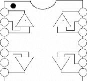
1
14
2
3
4
5
6
2 3
_ + _
+
_
1
+
+
_
4
12
11
13
10
9
7 8
OUT4
IN4 (-)
IN4 (+)
GND
IN3 (+)
IN3 (-)
OUT3
Rev. 1.0.3
Schematic Diagram
(One Section Only)
VCC
GND


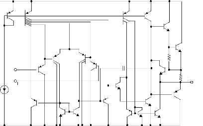
Q5 Q6
IN(-)
IN(+)
Q7
Q1
Q2
Q8
Q9
Q3
Q4
Q10
Q11
C1
Q13
Q12
Q14
Q17
Q15
Q18
Q16
Q19
R1
Q21
Q20
R2
OUTPUT
Absolute Maximum Ratings
Parameter
|
Symbol
|
LM224/LM224A
|
LM324/LM324A
|
LM2902
|
Unit
|
Power Supply Voltage
|
VCC
|
#177;16 or 32
|
#177;16 or 32
|
#177;13 or 26
|
V
|
Differential Input Voltage
|
VI(DIFF)
|
32
|
32
|
26
|
V
|
Input Voltage
|
VI
|
-0.3 to +32
|
-0.3 to +32
|
-0.3 to +26
|
V
|
Output Short Circuit to GND Vcc=15V, TA=25°C(one Amp)
|
-
|
Continuous
|
Continuous
|
Continuous
|
-
|
Power Dissipation, TA=25°C 14-DIP
14-SOP
|
PD
|
1310
640
|
1310
640
|
1310
640
|
mW
|
Operating Temperature Range
|
TOPR
|
-25 ~ +85
|
0 ~ +70
|
-40 ~ +85
|
°C
|
Storage Temperature Range
|
TSTG
|
-65 ~ +150
|
-65 ~ +150
|
-65 ~ +150
|
°C
|
|
Thermal Data
Parameter
|
Symbol
|
Value
|
Unit
|
Thermal Resistance Junction-Ambient Max.
|
|
|
|
14-DIP
|
Rèja
|
95
|
°C/W
|
14-SOP
|
|
195
|
|
|
Electrical Characteristics
(VCC = 5.0V, VEE = GND, TA = 25 LC, unless otherwise
specified)
Parameter
|
Symbol
|
Conditions
|
LM224
|
LM324
|
LM2902
|
Unit
|
|
Typ.
|
Max.
|
Min.
|
Typ.
|
Max.
|
Min.
|
Typ.
|
Max.
|
|
VIO
|
VCM = 0V to VCC -1.5V
VO(P) = 1.4V, RS
= 0LI
|
-
|
1.5
|
5.0
|
-
|
1.5
|
7.0
|
-
|
1.5
|
7.0
|
mV
|
Input Offset Current
|
IIO
|
-
|
-
|
2.0
|
30
|
-
|
3.0
|
50
|
-
|
3.0
|
50
|
nA
|
Input Bias Current
|
IBIAS
|
-
|
-
|
40
|
150
|
-
|
40
|
250
|
-
|
40
|
250
|
nA
|
Common-Mode Input
Voltage Range
|
VI(R)
|
Note1
|
0
|
-
|
VCC
-1.5
|
0
|
VCC
-1.5
|
-
|
0
|
-
|
VCC
-1.5
|
V
|
Supply Current
|
ICC
|
RL = L1,VCC = 30V (all Amps)
|
-
|
1.0
|
3
|
-
|
1.0
|
3
|
-
|
1.0
|
3
|
mA
|
|
-
|
0.7
|
1.2
|
-
|
0.7
|
1.2
|
-
|
0.7
|
1.2
|
mA
|
Large Signal
Voltage Gain
|
GV
|
VCC = 15V,RLL2KLI VO(P) = 1V to 11V
|
50
|
100
|
-
|
25
|
100
|
-
|
-
|
100
|
-
|
V/
mV
|
Output Voltage Swing
|
VO(H)
|
Note1
|
RL =
2KLI
|
26
|
-
|
-
|
26
|
-
|
-
|
22
|
-
|
-
|
V
|
|
27
|
28
|
-
|
27
|
28
|
-
|
23
|
24
|
-
|
V
|
|
VCC = 5V,RLL10KLI
|
-
|
5
|
20
|
-
|
5
|
20
|
-
|
5
|
100
|
mV
|
Common-Mode
Rejection Ratio
|
CMRR
|
-
|
70
|
85
|
-
|
65
|
75
|
-
|
50
|
75
|
-
|
dB
|
Power Supply Rejection Ratio
|
PSRR
|
-
|
65
|
100
|
-
|
65
|
100
|
-
|
50
|
100
|
-
|
dB
|
Channel Separation
|
CS
|
f = 1KHz to 20KHz
|
-
|
120
|
-
|
-
|
120
|
-
|
-
|
120
|
-
|
dB
|
Short Circuit to GND
|
ISC
|
-
|
-
|
40
|
60
|
-
|
40
|
60
|
-
|
40
|
60
|
mA
|
Output Current
|
ISOURCE
|
VI(+) = 1V, VI(-) = 0V VCC = 15V, VO(P)
= 2V
|
20
|
40
|
-
|
20
|
40
|
-
|
20
|
40
|
-
|
mA
|
|
VI(+) = 0V, VI(-) = 1V VCC = 15V, VO(P)
= 2V
|
10
|
13
|
-
|
10
|
13
|
-
|
10
|
13
|
-
|
mA
|
|
12
|
45
|
-
|
12
|
45
|
-
|
-
|
-
|
-
|
LA
|
Differential Input Voltage
|
VI(DIFF)
|
-
|
-
|
-
|
VCC
|
-
|
-
|
VCC
|
-
|
-
|
VCC
|
V
|
|
Note :
1. VCC=30V for LM224 and LM324 , VCC = 26V for LM2902
Electrical Characteristics (Continued)
(VCC = 5.0V, VEE = GND, unless otherwise specified)
The following specification apply over the range of -25°C =
TA = + 85°C for the LM224; and the 0°C = TA = +70°C for the
LM324 ; and the - 40°C = TA = +85°C for the LM2902
Parameter
|
Symbol
|
Conditions
|
LM224
|
LM324
|
LM2902
|
Unit
|
|
Typ.
|
Max.
|
Min.
|
Typ.
|
Max.
|
Min.
|
Typ.
|
Max.
|
|
VIO
|
VICM = 0V to VCC -1.5V
VO(P) = 1.4V, RS
= 0?
|
-
|
-
|
7.0
|
-
|
-
|
9.0
|
-
|
-
|
10.0
|
mV
|
Input Offset Voltage Drift
|
?VIO/?T
|
-
|
-
|
7.0
|
-
|
-
|
7.0
|
-
|
-
|
7.0
|
-
|
uV/°C
|
Input Offset Current
|
IIO
|
-
|
-
|
-
|
100
|
-
|
-
|
150
|
-
|
-
|
200
|
nA
|
Input Offset Current Drift
|
?IIO/?T
|
-
|
-
|
10
|
-
|
-
|
10
|
-
|
-
|
10
|
-
|
pA/°C
|
Input Bias Current
|
IBIAS
|
-
|
-
|
-
|
300
|
-
|
-
|
500
|
-
|
-
|
500
|
nA
|
Common-Mode Input Voltage Range
|
VI(R)
|
Note1
|
0
|
-
|
VCC
-2.0
|
0
|
-
|
VCC
-2.0
|
0
|
-
|
VCC
-2.0
|
V
|
Large Signal Voltage Gain
|
GV
|
VCC = 15V, RL = 2.0K?
VO(P) = 1V to 11V
|
25
|
-
|
-
|
15
|
-
|
-
|
15
|
-
|
-
|
V/mV
|
Output Voltage Swing
|
VO(H)
|
Note1
|
RL =
2K?
|
26
|
-
|
-
|
26
|
-
|
-
|
22
|
-
|
-
|
V
|
|
27
|
28
|
-
|
27
|
28
|
-
|
23
|
24
|
-
|
V
|
|
VCC = 5V,
RL=10K?
|
|
5
|
20
|
-
|
5
|
20
|
-
|
5
|
100
|
mV
|
Output Current
|
ISOURCE
|
VI(+) = 1V, VI(-) = 0V VCC = 15V, VO(P) = 2V
|
10
|
20
|
-
|
10
|
20
|
-
|
10
|
20
|
-
|
mA
|
|
VI(+) = 0V, VI(-) = 1V
VCC = 15V, VO(P) = 2V
|
10
|
13
|
-
|
5
|
8
|
-
|
5
|
8
|
-
|
mA
|
Differential Input Voltage
|
VI(DIFF)
|
-
|
-
|
-
|
VCC
|
-
|
-
|
VCC
|
-
|
-
|
VCC
|
V
|
|
Note:
1. VCC=30V for LM224 and LM324 , VCC = 26V for LM2902
Electrical Characteristics (Continued)
(VCC = 5.0V, VEE = GND, TA = 25LC, unless otherwise
specified)
Parameter
|
Symbol
|
Conditions
|
LM224A
|
LM324A
|
Unit
|
|
Typ.
|
Max.
|
Min.
|
Typ.
|
Max.
|
|
VIO
|
VCM = 0V to VCC -1.5V
VO(P) = 1.4V, RS = 0 u
|
-
|
1.0
|
3.0
|
-
|
1.5
|
3.0
|
mV
|
Input Offset Current
|
IIO
|
-
|
-
|
2
|
15
|
-
|
3.0
|
30
|
nA
|
Input Bias Current
|
IBIAS
|
-
|
-
|
40
|
80
|
-
|
40
|
100
|
nA
|
Input Common-Mode Voltage Range
|
VI(R)
|
VCC = 30V
|
0
|
-
|
VCC
-1.5
|
0
|
-
|
VCC
-1.5
|
V
|
Supply Current (All Amps)
|
ICC
|
VCC = 30V
|
-
|
1.5
|
3
|
-
|
1.5
|
3
|
mA
|
|
-
|
0.7
|
1.2
|
-
|
0.7
|
1.2
|
mA
|
Large Signal Voltage Gain
|
GV
|
VCC = 15V, RLL 2 Ku VO(P) = 1V to 11V
|
50
|
100
|
-
|
25
|
100
|
-
|
V/mV
|
Output Voltage Swing
|
VO(H)
|
Note1
|
RL = 2 Ku
|
26
|
-
|
-
|
26
|
-
|
-
|
V
|
|
RL = 10 Ku
|
27
|
28
|
-
|
27
|
28
|
-
|
V
|
|
VCC = 5V, RLL 10 Ku
|
-
|
5
|
20
|
-
|
5
|
20
|
mV
|
Common-Mode Rejection Ratio
|
CMRR
|
-
|
70
|
85
|
-
|
65
|
85
|
-
|
dB
|
Power Supply Rejection Ratio
|
PSRR
|
-
|
65
|
100
|
-
|
65
|
100
|
-
|
dB
|
Channel Separation
|
CS
|
f = 1KHz to 20KHz
|
-
|
120
|
-
|
-
|
120
|
-
|
dB
|
Short Circuit to GND
|
ISC
|
-
|
-
|
40
|
60
|
-
|
40
|
60
|
mA
|
Output Current
|
ISOURCE
|
VI(+) = 1V, VI(-) = 0V VCC = 15V
|
20
|
40
|
-
|
20
|
40
|
-
|
mA
|
|
VI(+) = 0V, VI(-) = 1V VCC = 15V, VO(P) = 2V
|
10
|
20
|
-
|
10
|
20
|
-
|
mA
|
|
12
|
50
|
-
|
12
|
50
|
-
|
LA
|
Differential Input Voltage
|
VI(DIFF)
|
-
|
-
|
-
|
VCC
|
-
|
-
|
VCC
|
V
|
|
Note:
1. VCC=30V for LM224A, LM324A
Electrical Characteristics (Continued)
(VCC = 5.0V, VEE = GND, unless otherwise specified)
The following specification apply over the range of -25°C =
TA = + 85°C for the LM224A; and the 0°C = TA = +70°C for the
LM324A
Parameter
|
Symbol
|
Conditions
|
LM224A
|
LM324A
|
Unit
|
|
Typ.
|
Max.
|
Min.
|
Typ.
|
Max.
|
|
VIO
|
VCM = 0V to VCC -1.5V VO(P) = 1.4V, RS = 0?
|
-
|
-
|
4.0
|
-
|
-
|
5.0
|
mV
|
Input Offset Voltage Drift
|
?VIO/?T
|
-
|
-
|
7.0
|
20
|
-
|
7.0
|
30
|
uV/°C
|
Input Offset Current
|
IIO
|
-
|
-
|
-
|
30
|
-
|
-
|
75
|
nA
|
Input Offset Current Drift
|
?IIO/?T
|
-
|
-
|
10
|
200
|
-
|
10
|
300
|
pA/°C
|
Input Bias Current
|
IBIAS
|
-
|
-
|
40
|
100
|
-
|
40
|
200
|
nA
|
Common-Mode Input Voltage Range
|
VI(R)
|
VCC = 30V
|
0
|
-
|
VCC
-2.0
|
0
|
-
|
VCC
-2.0
|
V
|
Large Signal Voltage Gain
|
GV
|
VCC = 15V, RL= 2.0K?
|
25
|
-
|
-
|
15
|
-
|
-
|
V/mV
|
Output Voltage Swing
|
VO(H)
|
VCC = 30V
|
RL = 2K?
|
26
|
-
|
-
|
26
|
-
|
-
|
V
|
|
27
|
28
|
-
|
27
|
28
|
-
|
|
|
VCC = 5V, RL= 10K?
|
-
|
5
|
20
|
-
|
5
|
20
|
mA
|
Output Current
|
ISOURCE
|
VI(+) = 1V, VI(-) = 0V VCC = 15V
|
10
|
20
|
-
|
10
|
20
|
-
|
mA
|
|
VI(+) = 0V, VI(-) = 1V VCC = 15V
|
5
|
8
|
-
|
5
|
8
|
-
|
mA
|
Differential Input Voltage
|
VI(DIFF)
|
-
|
-
|
-
|
VCC
|
-
|
-
|
VCC
|
V
|
|
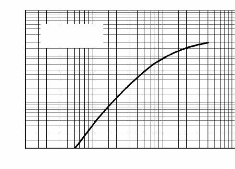
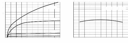
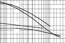
Typical Performance Characteristics
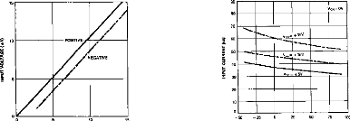
Supply Voltage(v) Temperature Tj ( °C)
Figure 1. Input Voltage Range vs Supply Voltage Figure
2. Input Current vs Temperature
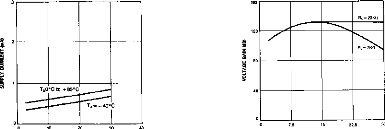
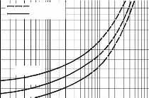
Supply Voltage (V)
Supply Voltage (V)
Figure 4. Voltage Gain vs Supply Voltage
Figure 3. Supply Current vs Supply Voltage
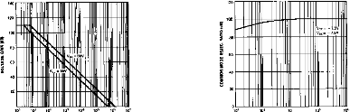
Frequency (Hz) Frequency (Hz)
Figure 5. Open Loop Frequency Response Figure 6. Common
mode Rejection Ratio
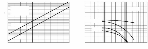
Typical Performance Characteristics
(Continued)
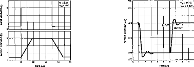
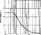
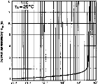
Figure 7. Slew Rate Figure 8. Voltage Follower Pulse
Response
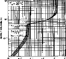
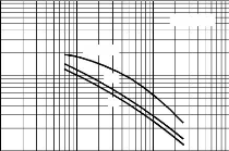
Figure 9. Large Signal Frequency Response Figure 10.
Output Characteristics vs Current Sourcing
Figure 11. Output Characteristics vs Current Sinking
Figure 12. Current Limiting vs Temperature
#1
#7
0.252 E0.008
6.40 E0.20
7.62
0.300
#14
#8
19.80 MAX 0.780
0.200
5.08
0.128 E0.008
3.25 E0.20
19.40 D0.20
0.764 D0.008
MAX
2.08
0.082
0.130 E0.012
3.30 E0.30
0.008
0.20
0.46 1110
0.018 LO.004
MIN
1.50 D0.10
0.059 LO.004
2.54
0.100
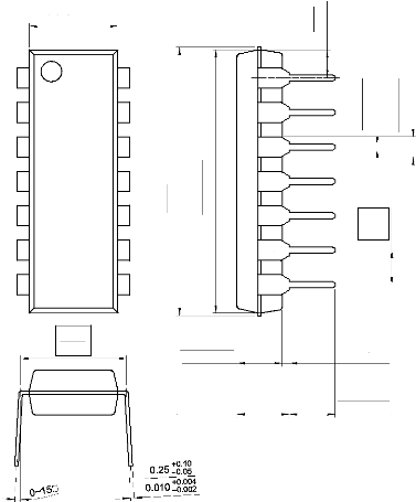
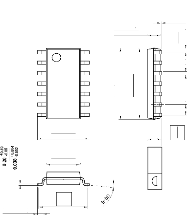
Mechanical Dimensions
Package
Dimensions in millimeters
14-DIP
Mechanical Dimensions (Continued)
Package
1.27
0.050
14-SOP
0.05
0.002
1.55 #177;0.10
0.061 #177;0.004
1.80 MAX 0.071
8.70
0.343 MAX
8.56 00.20
0.337 D0.008
3.95 #177;0.20
0.156 #177;0.008
0.60 #177;0.20
5.72
0.225
0.024 #177;0.008
0.019
0.47
(,,-..,, )
#1
#7
6.00 #177;0.30
0.236 #177;0.012
#8
#14
+0.10
-0.05
0.406
+0.004
-0.002
0.016
MIN
MAX0.10
MAX0.004
Dimensions in millimeters

GlobalOptoisolatorn
4N25
4N26
4N27
4N28


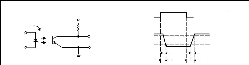
The 4N25, 4N26, 4N27 and 4N28 devices consist of a gallium
arsenide infrared emitting diode optically coupled to a monolithic silicon
phototransistor detector.
· Most Economical Optoisolator Choice for Medium Speed,
Switching Applications
· Meets or Exceeds All JEDEC Registered Specifications
·

6 1
STANDARD THRU HOLE
To order devices that are tested and marked per VDE
0884 requirements, the
suffix »V» must be included at end of part
number. VDE 0884 is a test option.
Applications
· General Purpose Switching Circuits
· Interfacing and coupling systems of different potentials
and impedances
· I/O Interfacing
· Solid State Relays
MAXIMUM RATINGS (TA = 25°C unless otherwise
noted)
INPUT LED
SCHEMATIC
PIN 1. LED ANODE
2. LED CATHODE
3. N.C.
4. EMITTER
5. COLLECTOR
6. BASE

1
2
3
6
5
4
Reverse Voltage
|
VR
|
3
|
Volts
|
|
Forward Current -- Continuous
|
IF
|
60
|
mA
|
|
LED Power Dissipation @ TA = 25°C
with Negligible Power in Output Detector Derate above
25°C
|
PD
|
120
1.41
|
mW
mW/°C
|
OUTPUT TRANSISTOR
|
Collector-Emitter Voltage
|
VCEO
|
30
|
Volts
|
|
Emitter-Collector Voltage
|
VECO
|
7
|
Volts
|
|
Collector-Base Voltage
|
VCBO
|
70
|
Volts
|
|
Collector Current -- Continuous
|
IC
|
150
|
mA
|
|
Detector Power Dissipation @ TA = 25°C with Negligible Power
in Input LED Derate above 25°C
|
PD
|
150
1.76
|
mW
mW/°C
|
TOTAL DEVICE
|
Isolation Surge Voltage(1)
(Peak ac Voltage, 60 Hz, 1 sec Duration)
|
VISO
|
7500
|
Vac(pk)
|
|
Total Device Power Dissipation @ TA = 25°C Derate above
25°C
|
PD
|
250
2.94
|
mW
mW/°C
|
|
Ambient Operating Temperature Range
|
TA
|
-55 to +100
|
°C
|
|
Storage Temperature Range
|
Tstg
|
-55 to +150
|
°C
|
|
Soldering Temperature (10 sec, 1/16? from case)
|
TL
|
260
|
°C
|
1. Isolation surge voltage is an internal device dielectric
breakdown rating. 1. For this test, Pins 1 and 2 are common, and Pins 4, 5 and
6 are common.
ELECTRICAL CHARACTERISTICS (TA = 25°C
unless otherwise noted)(1)
|
Characteristic
|
Symbol
|
Min
|
Typ(1)
|
Max
|
Unit
|
INPUT LED
|
Forward Voltage (IF = 10 mA) TA = 25°C
|
VF
|
--
|
1.15
|
1.5
|
Volts
|
|
TA = -55°C
|
|
--
|
1.3
|
--
|
|
|
TA = 100°C
|
|
--
|
1.05
|
--
|
|
|
Reverse Leakage Current (VR = 3 V)
|
IR
|
--
|
--
|
100
|
uA
|
|
Capacitance (V = 0 V, f = 1 MHz)
|
CJ
|
--
|
18
|
--
|
pF
|
OUTPUT TRANSISTOR
|
Collector-Emitter Dark Current 4N25,26,27
(VCE = 10 V, TA = 25°C 4N28
(VCE = 10 V, TA = 100°C) All Devices
|
ICEO
|
--
--
|
1
1
|
50
100
|
nA
|
|
ICEO
|
--
|
1
|
--
|
uA
|
|
Collector-Base Dark Current (VCB = 10 V)
|
ICBO
|
--
|
0.2
|
--
|
nA
|
|
Collector-Emitter Breakdown Voltage (IC = 1 mA)
|
V(BR)CEO
|
30
|
45
|
--
|
Volts
|
|
Collector-Base Breakdown Voltage (IC = 100 uA)
|
V(BR)CBO
|
70
|
100
|
--
|
Volts
|
|
Emitter-Collector Breakdown Voltage (IE = 100 uA)
|
V(BR)ECO
|
7
|
7.8
|
--
|
Volts
|
|
DC Current Gain (IC = 2 mA, VCE = 5 V)
|
hFE
|
--
|
500
|
--
|
--
|
|
Collector-Emitter Capacitance (f = 1 MHz, VCE = 0)
|
CCE
|
--
|
7
|
--
|
pF
|
|
Collector-Base Capacitance (f = 1 MHz, VCB = 0)
|
CCB
|
--
|
19
|
--
|
pF
|
|
Emitter-Base Capacitance (f = 1 MHz, VEB = 0)
|
CEB
|
--
|
9
|
--
|
pF
|
COUPLED
|
Output Collector Current (IF = 10 mA, VCE = 10 V)
4N25,26
4N27,28
|
IC (CTR)(2)
|
2 (20)
1 (10)
|
7 (70)
5 (50)
|
--
--
|
mA (%)
|
|
Collector-Emitter Saturation Voltage (IC = 2 mA, IF = 50 mA)
|
VCE(sat)
|
--
|
0.15
|
0.5
|
Volts
|
|
Turn-On Time (IF = 10 mA, VCC = 10 V, RL = 100 ?)(3)
|
ton
|
--
|
2.8
|
--
|
us
|
|
Turn-Off Time (IF = 10 mA, VCC = 10 V, RL = 100 ?)(3)
|
toff
|
--
|
4.5
|
--
|
us
|
|
Rise Time (IF = 10 mA, VCC = 10 V, RL = 100 ?)(3)
|
tr
|
--
|
1.2
|
--
|
us
|
|
Fall Time (IF = 10 mA, VCC = 10 V, RL = 100 ?)(3)
|
tf
|
--
|
1.3
|
--
|
us
|
|
Isolation Voltage (f = 60 Hz, t = 1 sec)(4)
|
VISO
|
7500
|
--
|
--
|
Vac(pk)
|
|
Isolation Resistance (V = 500 V)(4)
|
RISO
|
1011
|
--
|
--
|
?
|
|
Isolation Capacitance (V = 0 V, f = 1 MHz)(4)
|
CISO
|
--
|
0.2
|
--
|
pF
|
1. Always design to the specified minimum/maximum electrical
limits (where applicable).
2. Current Transfer Ratio (CTR) = IC/IF x 100%.
3. For test circuit setup and waveforms, refer to Figure 11.
4. For this test, Pins 1 and 2 are common, and Pins 4, 5 and 6
are common.
IF, LED INPUT CURRENT (mA)
IC, OUTPUT COLLECTOR CURRENT (NORMALIZED)
TYPICAL CHARACTERISTICS
TA = -55°C
25°C
100°C
PULSE ONLY PULSE OR DC
1 10 100 1000
2
VF, FORWARD VOLTAGE (VOLTS)
1.8
1.6
1.4
1.2
1
0.01 0.5 1
2 5 10 20 50
10
1
0.1
NORMALIZED TO:
IF = 10 mA
IF, LED FORWARD CURRENT (mA)
Figure 1. LED Forward Voltage versus Forward
Current
Figure 2. Output Current versus Input Current
VCE, COLLECTOR-EMITTER VOLTAGE (VOLTS)
-60 -40 -20 0 20 40 60 80 100
TA, AMBIENT TEMPERATURE (°C)
IC, OUTPUT COLLECTOR CURRENT (NORMALIZED)
IC, COLLECTOR CURRENT (mA)
28
24
20
16
12
4
8
0
2 mA
1 mA
0 1 2 3 4 5 6 7 8 9 10
IF = 10 mA
5 mA
1 0.7 0.5
0.2
0.1
10
2
7
5
NORMALIZED TO TA = 25°C
Figure 3. Collector Current versus Figure 4. Output
Current versus Ambient Temperature
Collector-Emitter Voltage
1
lac, COLLECTOR-EMITTER DARK CURRENT
(NORMALIZED)
0.1
00
10
1
NORMALIZED TO:
VCE = 10 V
TA = 25°C
VCE = 30 V
10 V
0 20 40 60 80 100
TA, AMBIENT TEMPERATURE (°C)
t, TIME (3)
100
50
20
10
5
2
1
0.1 0.2 0.5 1 2 5 10 20 50 100
IF, LED INPUT CURRENT (mA)
RL = 1000
RL = 100{
{
tf
tr
tr
tf
VCC = 10 V
Figure 5. Dark Current versus Ambient Temperature Figure
6. Rise and Fall Times
(Typical Values)
ton TURN--ON TIME (C)
100 70 50
20
10 7 5
2
1
RL = 1000
100
10
VCC = 10 V
0.1 0.2 0.5 0.7 1 2 5 7 10 20 50 70100
IF, LED INPUT CURRENT (mA)
Figure 7. Turn-On Switching Times
(Typical
Values)
IC ' TYPICAL COLLECTOR CURRENT (mA)
4
3
2
1
IF = 0
IB = 7 uA
4 uA
5 uA
3 uA
2 uA
1 uA
6 uA
0 2 4 6 8 10 12 14 16 18 20
VCE, COLLECTOR-EMITTER VOLTAGE (VOLTS)
toil TURN --OFF TIME (3)
100 70 50
20
10
7
5
2
1

RL = 1000
100
10
VCC = 10 V
0.1 0.2 0.5 0.7 1 2 5 7 10 20 50 70100
IF, LED INPUT CURRENT (mA)
Figure 8. Turn-Off Switching Times
(Typical
Values)
C, CAPACITANCE (pF)
20
18
16
14
12
10
8
6
4
2
0
CLED
CCB
CCE
CEB
f = 1 MHz
0.05 0.1 0.2 0.5 1 2 5 10 20 50
V, VOLTAGE (VOLTS)
TEST CIRCUIT
VCC = 10 V
WAVEFORMS
IF = 10 mA
RL = 100 ?
INPUT
OUTPUT
90%
tr
ton
tf toff
INPUT PULSE
10%
OUTPUT PULSE
Figure 9. DC Current Gain (Detector Only) Figure 10.
Capacitances versus Voltage
PACKAGE DIMENSIONS
0.13 (0.005)
M
NOTES:
1. DIMENSIONING AND TOLERANCING PER ANSI Y14.5M, 1982.
2. CONTROLLING DIMENSION: INCH.
3. DIMENSION L TO CENTER OF LEAD WHEN FORMED PARALLEL.
|
DIM
|
INCHES
|
MILLIMETERS
|
|
MIN
|
MAX
|
MIN
|
MAX
|
|
A
|
0.320
|
0.350
|
8.13
|
8.89
|
|
B
|
0.240
|
0.260
|
6.10
|
6.60
|
|
C
|
0.115
|
0.200
|
2.93
|
5.08
|
|
D
|
0.016
|
0.020
|
0.41
|
0.50
|
|
E
|
0.040
|
0.070
|
1.02
|
1.77
|
|
F
|
0.010
|
0.014
|
0.25
|
0.36
|
|
G
|
0.100 BSC
|
2.54 BSC
|
|
J
|
0.008
|
0.012
|
0.21
|
0.30
|
|
K
|
0.100
|
0.150
|
2.54
|
3.81
|
|
L
|
0.300 BSC 7.62 BSC
|
|
M
|
0
|
15
|
0
|
15
|
|
N
|
0.015
|
0.100
|
0.38
|
2.54
|
STYLE 1:
PIN 1. ANODE
2. CATHODE
3. NC
4. EMITTER
5. COLLECTOR
6. BASE
THRU HOLE
6 4
1 3
-A-
-B-
C
K
L
J 6 PL
M
0.13 (0.005)
M
T
G
D
6 PL
-T-
SEATING PLANE
E 6 PL
F 4 PL
N
B
M
A M
T
A
M
B M
NOTES:
1. DIMENSIONING AND TOLERANCING PER ANSI Y14.5M, 1982.
2. CONTROLLING DIMENSION: INCH.
|
INCHES
|
MILLIMETERS
|
|
DIM
|
MIN
|
MAX
|
MIN
|
MAX
|
|
A
|
0.320
|
0.350
|
8.13
|
8.89
|
|
B
|
0.240
|
0.260
|
6.10
|
6.60
|
|
C
|
0.115
|
0.200
|
2.93
|
5.08
|
|
D
|
0.016
|
0.020
|
0.41
|
0.50
|
|
E
|
0.040
|
0.070
|
1.02
|
1.77
|
|
F
|
0.010
|
0.014
|
0.25
|
0.36
|
|
G
|
0.100 BSC
|
2.54 BSC
|
|
H
|
0.020
|
0.025
|
0.51
|
0.63
|
|
J
|
0.008
|
0.012
|
0.20
|
0.30
|
|
K
|
0.006
|
0.035
|
0.16
|
0.88
|
|
L
|
0.320 BSC
|
8.13 BSC
|
|
S
|
0.332 0.390
|
8.43 9.90
|
SURFACE MOUNT
6 4
1
-A-
3
-B-
B
M
E 6 PL
F 4 PL
G
D 6 PL
0.13 (0.005)
H
C
M
T
A
M
B M
L
K 6 PL
0.13 (0.005)
J
M
-T-
SEATING PLANE
T
A M
4N25 4N26 4N27 4N28
NOTES:
1. DIMENSIONING AND TOLERANCING PER ANSI Y14.5M, 1982.
2. CONTROLLING DIMENSION: INCH.
3. DIMENSION L TO CENTER OF LEAD WHEN FORMED PARALLEL.
|
INCHES
|
MILLIMETERS
|
|
DIM
|
MIN
|
MAX
|
MIN
|
MAX
|
|
A
|
0.320
|
0.350
|
8.13
|
8.89
|
|
B
|
0.240
|
0.260
|
6.10
|
6.60
|
|
C
|
0.115
|
0.200
|
2.93
|
5.08
|
|
D
|
0.016
|
0.020
|
0.41
|
0.50
|
|
E
|
0.040
|
0.070
|
1.02
|
1.77
|
|
F
|
0.010
|
0.014
|
0.25
|
0.36
|
|
G
|
0.100 BSC
|
2.54 BSC
|
|
J
|
0.008
|
0.012
|
0.21
|
0.30
|
|
K
|
0.100
|
0.150
|
2.54
|
3.81
|
|
L
|
0.400
|
0.425
|
10.16
|
10.80
|
|
N
|
0.015
|
0.040
|
0.38
|
1.02
|
0.4" LEAD SPACING
D 6 PL
6 4
1 3
-A-
G
N
-B-
K
C
L
J
F 4 PL
-T-
SEATING
PLANE
E 6 PL
T
A
B M
M
M
0.13 (0.005)
PowerMOS transistor IRF840
Avalanche energy rated
FEATURES SYMBOL QUICK REFERENCE DATA
·
d
s
VDSS = 500 V
ID = 8.5 A
RDS(ON) = 0.85 Ù
Repetitive Avalanche Rated
· Fast switching
· High thermal cycling performance
· Low thermal resistance
GENERAL DESCRIPTION PINNING SOT78 (TO220AB)
N-channel, enhancement mode field-effect power transistor,
intended for use in off-line switched mode power supplies, T.V. and computer
monitor power supplies, d.c. to d.c. converters, motor control circuits and
general purpose switching applications.
The IRF840 is supplied in the SOT78 (TO220AB) conventional
leaded package.
|
PIN
|
DESCRIPTION
|
|
1
2
3
tab
|
gate drain source
drain
|
|
tab
|
|
1 2 3
LIMITING VALUES
Limiting values in accordance with the Absolute Maximum System
(IEC 134)
|
SYMBOL
|
PARAMETER
|
CONDITIONS
|
MIN.
|
MAX.
|
UNIT
|
|
VDSS
|
Drain-source voltage
|
Tj = 25 °C to 150°C
|
-
|
500
|
V
|
|
VDGR
|
Drain-gate voltage
|
Tj = 25 °C to 150°C; RGS = 20 kÙ
|
-
|
500
|
V
|
|
VGS
|
Gate-source voltage
|
|
-
|
#177; 30
|
V
|
|
ID
|
Continuous drain current
|
Tmb = 25 °C; VGS = 10 V
|
-
|
8.5
|
A
|
|
|
Tmb = 100 °C; VGS = 10 V
|
-
|
5.4
|
A
|
|
IDM
|
Pulsed drain current
|
Tmb = 25 °C
|
-
|
34
|
A
|
|
PD
|
Total dissipation
|
Tmb = 25 °C
|
-
|
147
|
W
|
|
Tj, Tstg
|
Operating junction and storage temperature range
|
|
- 55
|
150
|
°C
|
AVALANCHE ENERGY LIMITING VALUES
Limiting values in accordance with the Absolute Maximum System
(IEC 134)
|
SYMBOL
|
PARAMETER
|
CONDITIONS
|
MIN.
|
MAX.
|
UNIT
|
|
EAS
|
Non-repetitive avalanche energy
|
Unclamped inductive load, IAS = 7.4 A;
tp = 0.22 ms; Tj prior to avalanche = 25°C;
|
-
|
531
|
mJ
|
|
|
VDD = 50 V; RGS = 50 Ù; VGS = 10 V; refer to fig:17
|
|
|
|
|
EAR
|
Repetitive avalanche energy1
|
IAR = 8.5 A; tp = 2.5 ìs; Tj prior to
avalanche = 25°C; RGS = 50 Ù; VGS = 10 V; refer to
fig:18
|
-
|
13
|
mJ
|
|
IAS, IAR
|
Repetitive and non-repetitive avalanche current
|
|
-
|
8.5
|
A
|
1 pulse width and repetition rate limited by Tj
max.
PowerMOS transistor IRF840
Avalanche energy rated
THERMAL RESISTANCES
|
SYMBOL
|
PARAMETER
|
CONDITIONS
|
MIN.
|
TYP.
|
MAX.
|
UNIT
|
|
Rth j-mb Rth j-a
|
Thermal resistance junction to mounting base
Thermal resistance junction to ambient
|
in free air
|
-
-
|
-
60
|
0.85
-
|
K/W
K/W
|
ELECTRICAL CHARACTERISTICS
Tj = 25 °C unless otherwise specified
|
SYMBOL
|
PARAMETER
|
CONDITIONS
|
MIN.
|
TYP.
|
MAX.
|
UNIT
|
|
V(BR)DSS
|
Drain-source breakdown voltage
|
VGS = 0 V; ID = 0.25 mA
|
500
|
-
|
-
|
V
|
|
ÄV(BR)DSS / ÄTj
|
Drain-source breakdown voltage temperature coefficient
|
VDS = VGS; ID = 0.25 mA
|
-
|
0.1
|
-
|
%/K
|
|
RDS(ON)
|
Drain-source on resistance
|
VGS = 10 V; ID = 4.8 A
|
-
|
0.6
|
0.85
|
Ù
|
|
VGS(TO)
|
Gate threshold voltage
|
VDS = VGS; ID = 0.25 mA
|
2.0
|
3.0
|
4.0
|
V
|
|
gfs
|
Forward transconductance
|
VDS = 30 V; ID = 4.8 A
|
3.5
|
6
|
-
|
S
|
|
IDSS
|
Drain-source leakage current
|
VDS = 500 V; VGS = 0 V
|
-
|
1
|
25
|
ìA
|
|
|
VDS = 400 V; VGS = 0 V; Tj = 125 °C
|
-
|
40
|
250
|
ìA
|
|
IGSS
|
Gate-source leakage current
|
VGS = #177;30 V; VDS = 0 V
|
-
|
10
|
200
|
nA
|
|
Qg(tot)
|
Total gate charge
|
ID = 8.5 A; VDD = 400 V; VGS = 10 V
|
-
|
55
|
80
|
nC
|
|
Qgs
|
Gate-source charge
|
|
-
|
5.5
|
7
|
nC
|
|
Qgd
|
Gate-drain (Miller) charge
|
|
-
|
30
|
45
|
nC
|
|
td(on)
|
Turn-on delay time
|
VDD = 250 V; RD = 30 Ù;
|
-
|
18
|
-
|
ns
|
|
tr
|
Turn-on rise time
|
RG = 9.1 Ù
|
-
|
37
|
-
|
ns
|
|
td(off)
|
Turn-off delay time
|
|
-
|
80
|
-
|
ns
|
|
tf
|
Turn-off fall time
|
|
-
|
36
|
-
|
ns
|
|
Ld
|
Internal drain inductance
|
Measured from tab to centre of die
|
-
|
3.5
|
-
|
nH
|
|
Ld
|
Internal drain inductance
|
Measured from drain lead to centre of die
|
-
|
4.5
|
-
|
nH
|
|
Ls
|
Internal source inductance
|
Measured from source lead to source bond pad
|
-
|
7.5
|
-
|
nH
|
|
Ciss
|
Input capacitance
|
VGS = 0 V; VDS = 25 V; f = 1 MHz
|
-
|
960
|
-
|
pF
|
|
Coss
|
Output capacitance
|
|
-
|
140
|
-
|
pF
|
|
Crss
|
Feedback capacitance
|
|
-
|
80
|
-
|
pF
|
SOURCE-DRAIN DIODE RATINGS AND
CHARACTERISTICS
Tj = 25 °C unless otherwise specified
|
SYMBOL
|
PARAMETER
|
CONDITIONS
|
MIN.
|
TYP.
|
MAX.
|
UNIT
|
|
IS
|
Continuous source current
|
Tmb = 25°C
|
-
|
-
|
8.5
|
A
|
|
(body diode)
|
|
|
|
|
|
|
ISM
|
Pulsed source current (body diode)
|
Tmb = 25°C
|
-
|
-
|
34
|
A
|
|
VSD
|
Diode forward voltage
|
IS = 8.5 A; VGS = 0 V
|
-
|
-
|
1.2
|
V
|
|
trr
|
Reverse recovery time
|
IS = 8.5 A; VGS = 0 V; dI/dt = 100 A/ìs
|
-
|
440
|
-
|
ns
|
|
Qrr
|
Reverse recovery charge
|
|
-
|
6.4
|
-
|
ìC
|
120 110 100 90 80 70 60 50 40 30 20 10
0
Fig.1. Normalised power dissipation.
PD% = 100·PD/PD 25 °C = f(Tmb)
0 20 40 60 80 100 120 140
Tmb / C
PD% Normalised Power Derating
120 110 100 90 80 70 60 50 40 30 20 10
0
Fig.2. Normalised continuous drain current.
ID% =
100·ID/ID 25 °C = f(Tmb); conditions: VGS
= 10 V
0 20 40 60 80 100 120 140
Tmb / C
ID% Normalised Current Derating
ID / A
100
10
DC
1
100 ms
0.1
Fig.3. Safe operating area. Tmb = 25
°C
ID & IDM = f(VDS); IDM single pulse; parameter
tp
1 10 100 1000
VDS / V
tp = 10 us
100 us 1 ms
10 ms
ID, Drain current (Amps
|
Tj = 25 C
|
|
|
|
|
10 V
|
|
|
|
|
7 V
|
6.5 V
|
|
|
6 V
|
|
|
|
|
|
5.5 V
|
|
|
|
|
|
5 V
|
|
|
|
|
= 4.5 V
|
|
|
|
|
VGS
|
|
|
|
|
|
|
0 5 10 15 20 25 30
VDS, Drain-Source voltage (Volts)
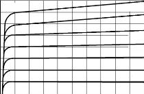
Fig.5. Typical output characteristics.
ID =
f(VDS); parameter VGS
30
25
20
15
10
5
0
RDS(on), Drain-Source on resistance (Ohms
|
4.5 V
|
|
|
5 V
|
5.5 V
|
VGS = 6 V
|
Tj = 25 C
|
|
|
|
|
|
|
6.5 V
7 V
10 V
|
|
|
|
|
|
0 5 10 15 20 25
ID, Drain current (Amps)
Fig.6. Typical on-state resistance.
RDS(ON) =
f(ID); parameter VGS
2
1.5
1
0.5
0
D = 0.5
0.2
0.1
0.1
0.05
0.02
0.01
tp D = tp
T
PD
single pulse
t
T
1ms 10ms 100ms 1s
tp, pulse width (s)
0.0011us 10us 100us
1 Zth j-mb, Transient thermal impedance (K/W)
Fig.4. Transient thermal impedance.
Zth j-mb = f(t);
parameter D = tiT
PowerMOS transistor IRF840
Avalanche energy rated
ID, Drain current (Amps)
25
VDS > ID x RDS(on)max
20
15
10
5
Tj = 150 C
Tj = 25 C
0
0 2 4 6 8 10
Fig.7. Typical transfer characteristics.
ID = f(VGS);
parameter Tj
VGS, Gate-Source voltage (Volts)
gfs, Transconductance (S)
10
VDS > ID x RDS(on)max
Tj = 25 C
8
150 C
6
4
2
0
ID, Drain current (A)
0 5 10 15 20 25
Fig.8. Typical transconductance.
gfs = f(ID);
parameter Tj
Normalised RDS(ON) = f(Tj)
a
2
1
0
Fig.9. Normalised drain-source on-state resistance.
a = RDS(ON)/RDS(ON)25 °C = f(Tj); ID = 4.25 A; VGS =
10 V
-60 -40 -20 0 20 40 60 80 100 120 140
Tj / C
VGS(TO) / V
max.
typ.
4
3
min.
2
1
Fig.10. Gate threshold voltage.
VGS(TO) =
f(Tj); conditions: ID = 0.25 mA; VDS = VGS
0
-60 -40 -20 0 20 40 60 80 100 120 140
Tj / C
SUB-THRESHOLD CONDUCTION
ID / A
1E-01
1E-02
2 %
typ
98 %
1E-03
1E-04
1E-05
1E-06
Fig.11. Sub-threshold drain current.
ID = f(VGS);
conditions: Tj = 25 °C; VDS = VGS
0 1 2 3 4
VGS / V
Junction capacitances (pF)
10000
Ciss
1000
Coss
100
Crss
10
Fig.12. Typical capacitances, Ciss, Coss, Crss. C =
f(VDS); conditions: VGS = 0 V; f = 1 MHz
1 10 100 1000
VDS, Drain-Source voltage (Volts)
PowerMOS transistor IRF840
Avalanche energy rated
PowerMOS transistor IRF840
Avalanche energy rated
PHP8N50E
15
ID = 8.5A Tj = 25 C
14
13
200V
12
11
10
100V
9
8
VDD = 400 V
7
6
5
4
3
2
1
0
Gate-source voltage, VGS (V)
IF, Source-Drain diode current (Amps)
VGS = 0 V
Tj = 25 C
5
0
20
10
150 C
Fig.13. Typical turn-on gate-charge characteristics.
VGS
= f(QG); parameter VDS
0 20 40 60 80
Gate charge, QG (nC)
Switching times (ns)
1000
VDD = 250 V
VGS = 10 V
RD = 30 Ohms
Tj = 25 C
td(off)
100
tf
tr
td(on)
10
RG, Gate resistance (Ohms)
Fig.14. Typical switching times;
td(on), tr,
td(off), tf = f(RG)
0 10 20 30 40 50 60
1.15
V(BR)DSS @ Tj
V(BR)DSS @ 25 C
1.1
1.05
1
0.95
0.9
0.85
Tj, Junction temperature (C)
Fig.15. Normalised drain-source breakdown voltage;
V(BR)DSS/V(BR)DSS 25 °C = f(Tj)
100 50 0 50 100 150
Normalised Drain-source breakdown voltage
0 0.2 0.4 0.6 0.8 1 1.2 1.4
VSDS, Source-Drain voltage (Volts)
10
25 C
Tj prior to avalanche = 125 C
1
0.1
Fig.17. Maximum permissible non-repetitive
avalanche
current (IAS) versus avalanche time (tp);
unclamped
inductive load
1E-06 1E-05 1E-04 1E-03 1E-02
Avalanche time, tp (s)
Non-repetitive Avalanche current, IAS (A)
10
Tj prior to avalanche = 25 C
125 C
1
0.1
PHP8N50E
0.01
Fig.18. Maximum permissible repetitive avalanche
current
(IAR) versus avalanche time (tp)
1E-06 1E-05 1E-04 1E-03 1E-02
Avalanche time, tp (s)
Maximum Repetitive Avalanche Current, IAR (A)
Fig.16. Source-Drain diode characteristic. IF =
f(VSDS); parameter Tj
PowerMOS transistor IRF840
Avalanche energy rated
MECHANICAL DATA
Plastic single-ended package; heatsink mounted; 1
mounting hole; 3-lead TO-220 SOT78


L2(1)
b1
D1
e e
1
2
3
b
L1
q
0 5 10 mm

scale
DIMENSIONS (mm are the original dimensions)
|
UNIT
|
A
|
A1
|
b
|
b1
|
c
|
D
|
D1
|
E
|
e
|
L
|
L1
|
(1) L2 max.
|
P
|
q
|
Q
|
|
mm
|
4.5
4.1
|
1.39
1.27
|
0.9
0.7
|
1.3
1.0
|
0.7
0.4
|
15.8
15.2
|
6.4
5.9
|
10.3
9.7
|
2.54
|
15.0
13.5
|
3.30
2.79
|
3.0
|
3.8
3.6
|
3.0
2.7
|
2.6
2.2
|
Note
1. Terminals in this zone are not tinned.
|
OUTLINE
VERSION
|
REFERENCES
|
EUROPEAN
PROJECTION
|
ISSUE DATE
|
|
IEC
|
JEDEC
|
EIAJ
|
|
|
SOT78
|
|
TO-220
|
|
|
|
97-06-11
|
|
c
A
A1
Q
Fig.19. SOT78 (TO220AB); pin 2 connected to mounting base
(Net mass:2g)
Notes
1. This product is supplied in anti-static packaging. The
gate-source input must be protected against static discharge during transport
or handling.
2. Refer to mounting instructions for SOT78 (TO220AB)
package.
3. Epoxy meets UL94 V0 at 1/8".


[1] GLAISE Christian. "Introduction à
l'Électrotechnique et à l'Électronique de puissance".
Collection médiathèque e-EEA du club EEA. Version du 9 septembre
2002. Disponible sur le site
http://www.geii.iut-nimes.fr/cg/
de l'IUT de Nîmes.
[3] GASTON Bachelard in "la Formation de
l'esprit scientifique" , les composants d'électronique de puissance.
Version du septembre 2004.
[3]. MOUSTAFAOUI Dris, OUAGUENI
Abdelmadjid, "Étude comparative de différentes
stratégies de commande des variateurs de vitesse", Mémoire de fin
d'étude cycle licence département d'électrotechnique,
université de M'sila 2009, dirigé par: Mr : KHODJA Djalal
Eddine.
[4] MAARAD Samir, BELKHIRI Walid,
"Maintenance des maquettes didactiques de l'électronique de puissance".
Mémoire de fin d'étude cycle ingénieur département
d'électrotechnique, université de Batna 2010, dirigé par
Ms : KERCHA Mbarka.
[6]
www.google.com,
ChapitreII_Les_interrupteurs_semi_conducteurs.pdf.
[8] Cours Énergie et convertisseurs d'énergie,
"Chapitre 2 interrupteurs semi-conducteurs de puissance", Université de
Savoie Licence EEA.
[10] ACHORA Atef, HAMDI Farid, "Étude et
réalisation d'une maquette d'un hacheur série à base d'une
MOSFET", Mémoire de fin d'étude cycle DUEA département
d'électrotechnique, université de Batna, dirigé par
Mr:
Bendaas Med Lokman.
[8] Cours d'électronique de puissance de
4éme année machine de Mr : Bendaas Med Lokman.
[9]

[11] http : //
ww.pwrx.com.
[12]
www.google.com,
cours_hacheurs.pdf.
[13] http : //
validator.w3.org.
[14]
www.google.com,
cours_hacheur4-quadrants.
[16] RAHMOUNI Abderrezak , "Commande d'un
moteur à courant continu (assistée par le PIC16F84)".
Mémoire de fin d'étude cycle ingénieur département
d'électrotechnique, université de Batna 2004, dirigé par
Mr : A.H-Haddoun et Mr : S.Drid.
[18] DRAIFA Samir, MEBARKIA Abderaouf,
"Étude et réalisation d'une maquette didactique pour
l'électronique de puissance (Redresseur - Gradateur - Hacheur)",
Mémoire de fin d'étude cycle ingénieur département
d'électrotechnique, université de Batna 2008, dirigé par
Mr : Bendaas Med Lokman.
[20] LAIB Hichem, BAIDI Badiss,
"Étude et réalisation d'une carde de commande d'un thyristor et
d'un hacheur". Mémoire de fin d'étude cycle ingénieur
département d'électrotechnique, université de Batna 2005,
dirigé par Mr : Bendaas Med Lokman.
http : //
www.eupec.com.
[10] BOUKRANA Lilia, "Étude et
réalisation d'un hacheur réversible en tension", Mémoire
de fin d'étude cycle DUEA département d'électrotechnique,
université de Batna 2008, dirigé par Mr. Bendaas Med
Lokman.
|