3.1.4. Duration of evacuation process
The evacuation process of a vacuum system is generally
non-stationary. During evacuation, the pressure and flow of each point of the
installation vary. The evacuation duration is the time it takes to obtain a
certain pressure in the vacuum installation.
For a piping with high conductance, we'll have:
V
??= ?? ????(??0 ?? ) (3.15)
V : The chamber volume (m3);
36
Chapter 3: Vapor deposition and thin layer
characterization techniques
P0 : The pressure of the gas at the initial instant
(N/??2);
P : The pressure of the evacuated gas
(N/??2).
In the general case, the pumping time can be obtained using
the nomogram shown in figure 3.4. To use it, first calculate the quotient V/??
by joining the points corresponding to V and Q on the respective straight
lines. The obtained point on the line V/?? is joined to the point of the line P
which corresponds to the pressure P which we wish to obtain. The point of
intersection on the line t gives the necessary pumping time.
??/??
Fig.3.4 Nomogram for calculating the pumping time
3.2. The theory of plasmas
In their normal state, gases are electrical insulators. This
is due to the fact that they don't contain free charged particles, but only
neutral molecules. However, if they are given fairly strong electric fields,
they become conductors. The phenomena that occur are called discharges in gases
and are due to the appearance of electrons and free ions. The result of a
discharge in a gas is the production of an ionized gas.
The degree of ionization of a gas is defined by the ratio
á:
n
?? = (3.16)
n0 + n
n0 : The number of neutral particles per unit of volume;
n : The number of ionized particles per unit of volume.
The degree of ionization value varies from very low values (of
the order 10-10) to one. When the degree of ionization is equal to
unity, it is said that the gas is totally ionized or that it constitutes
plasma.
37
Chapter 3: Vapor deposition and thin layer
characterization techniques
The set of concepts, methods and results of the study of this
state of matter constitutes the physics of plasmas. In our environment, the
plasma phase is totally absent in the natural state, whereas on the cosmic
scale, more than 99.9% of the visible matter occurs in this phase.
When heating a gas at a sufficiently high temperature (of the
order of 104 K), the mean translated energy of its
molecules can become of the same order as their ionization energy. Under these
conditions, when two molecules collide, one of them can be ionized.
The probability of ionization as a function of energy is
characterized by a threshold. This is the ionization energy. The ionization
energies for all species are found in data banks.
Among all the weakly ionized gases we distinguish three
families:
- Lowly ionized gases: in which some ions and electrons move
in the middle of a sea of neutral molecules. Ions and electrons interact only
with neutral molecules;
- Highly ionized gases without interactions between particles:
in this plasma the charged particles follow without any collision a trajectory
determined by external electromagnetic fields; - Highly ionized gases with
interactions between particles.
Coating with plasma involves of modifying the state the
surface by one of the three following methods:
- The deposition on the surface a thin layer of a few
material;
- Chemical reaction with the surface itself (oxidation,
nitriding) or physicochemical transformation thereof (modification of adhesion,
surface energy);
- Erosion of the surface either by chemical action (formation
of pores between one or more atoms of the surface) or ion sputtering due to
plasma ion bombardment of the surface atoms or chemically-assisted sputtering,
which combines ion bombardment and chemical erosion.
The main types of plasma are: hot plasma and cold plasma.
The plasma is called «hot» when the temperature of
the ions and electrons is high (greater than 107 k ). In
this case, the medium is completely ionized.
The plasma is called «cold» when the electrons are
hot (on the order of 104 k), and the ions are cold (from
300 to 104 k). The medium in this case is weakly ionized
(ionization rate is close to 10-6 until 10-2
per neutral species).
3.3. Coating in the vapor phase (PVD, CVD)
Vapor deposition techniques allow us to have a deposit of thin
layers (generally less than 10ìm) with very interesting physical and
mechanical characteristics. Generally we distinguish two methods of deposition
from the vapor phase: physical vapor deposition (PVD) and chemical vapor
deposition (CVD).
In PVD processes, evaporation, sublimation or sputtering by
ionic bombardment are used to transform the material of deposition in the vapor
phase. These vapors are then condensed on the surfaces. The process can be
summarized by the formula:
???????? s??l??d ??????s
??????s ??????ld s??l??d
38
Chapter 3: Vapor deposition and thin layer
characterization techniques
The absence of a chemical reaction gave the designation:
physical deposition.
In CVD, one or more vapors (two in general) are used,
which react with each other on a surface to form a defined compound and
volatile products of the reaction:
AG + BGas + hot surface Csolide + DGas
+ "'
The various processes of the PVD and CVD techniques are
given in Table 3.2
|
Chemical vapor deposition(CVD)
|
Physical vapor deposition (PVD)
|
|
- Conventional chemical vapor deposition (CVD) -
Metalorganic chemical vapor deposition (MOCVD)
- Plasma-enhanced chemical vapor deposition
(PECVD)
|
- physical vapor deposition by evaporation: - PVD by
direct evaporation
- PVD by Ionic deposition
- physical vapor deposition by sputtering
|
Table 3.2 Various processes of the PVD and CVD
3.3.1. Chemical vapor deposition (CVD) techniques
3.3.1.1. Conventional chemical vapor deposition (CVD)
Two processes can be distinguished according to the
gaseous environment:
- Static processes:
It is an isothermal process, in which the bar to be
coated is placed in a closed chamber in contact with a mixture of a donor
eventually alloyed (metal powder containing the element to be deposited), an
activator (halogen compound) and an inert diluent which avoids self-sintering
of the assembly. At 400 ° C, the activator reacts with the donor element
to form the metal vapor. The subsequent heating at temperature between 800
° C and 1100 ° C under a hydrogen atmosphere allows ensuring the
production of the coating in a homogeneous manner.
- Dynamic processes:
For this process, the environment of the bar to be
coated is continuously renewed by the circulation of a gaseous mixture of the
material of the deposition formed outside the reaction chamber and carried by
forced convection on the surface of the bar.
The need for high temperature in conventional chemical
deposits to initiate the different chemical reactions leading to the metal
transfer, several paths has been followed to do so, and two are the most
developed for industry: the use of organic gaseous species (OMCVD) and the
assistance of plasma (PACVD).
3.3.1.2. Metalorganic chemical vapor deposition
(MOCVD)
The idea is to reduce the temperature of the
conventional CVD by substituting the halogenated compounds which have a higher
decomposition temperature than the new organometallic compounds.
The advantage of such a process is the lowering of the
processing temperature compared with conventional CVD processes, taking the
example of chromium deposition, the temperature is
39
Chapter 3: Vapor deposition and thin layer
characterization techniques
reduced from 1000 °C for the conventional CVD to 500
°C using by bis-benzene chrome Cr(C6H6)2, the rupture of the radical
bonding results in the formation of chromium carbide.
On the other hand, the disadvantages of this process are: the
high cost, the toxicity for a large number of them and the lack of stability
over time.
Electronics is the most favorable field for the development of
the OMCVD technique, with layers of some ten of nanometers.
3.3.1.3. Plasma-enhanced chemical vapor deposition
(PACVD)
A second way to reduce the temperature of the deposit to avoid
any further heat treatment (see table 3.3), is to use the assistance of plasma
and the use of chemically activated species such as ions and free radicals.
These species are produced in the gaseous phase by electron-molecule
collisions; the assistance of a plasma allows to obtain deposition speed
varying from 1 to a few tens of ìm/h in a temperature range comprised
between 150 and 500 ° C.
|
Deposition temperature (°C)
|
|
materiel
|
CVD
|
PACVD
|
|
Tungsten carbonate
|
1000
|
325-525
|
|
Poly silicon
|
650
|
200-400
|
|
Silicon nitride
|
900
|
300
|
|
Silicon dioxide
|
800-1100
|
300
|
|
Titanium Carbide
|
900-1100
|
500
|
|
Nitride of titanium
|
900-1100
|
500
|
Table 3.3 Typical temperature of deposition for CVD and
PECVD
3.3.2. Physical vapor deposition Processes
(PVD)
The PVD technique consists of the formation of a coating under
reduced pressure in three distinct stages: vaporization of the species to be
deposited, transport of these species and finally the condensation and the
growth of the deposit. There are two main processes of this technique, those
using evaporation and those using sputtering.
3.3.2.1. Physical vapor deposition by direct
evaporation
Evaporated species (atoms, molecules) propagate in a straight
line and condense on the cold zone (see figure 3.5). The transfer of the
species takes place in molecular flow under a pressure of less than
10-2 mbar, the rate of evaporation of the atoms can be found by the
hertz-knudsen equation:
??(??) = av ??
2??R?? (P??- P) (3.17)
a: Stricking coefficient, it is the probability of
having an adsorption; P: Gas pressure;
P??: Saturated vapor pressure;
R: Ideal gas constant.
40
Chapter 3: Vapor deposition and thin layer
characterization techniques
The advantages of this process are:
- High deposition rates (more than 200 ìm / h);
- Low processing temperature allowing deposits on plastic.
The disadvantage of this process is that the deposits have a
weak adherence and are often powdery, because they are made in a vapor phase
with a low energy. It is often necessary to heat the substrate towards 300 to
400 °C, or to use subsequent heat treatments to improve the adhesion.
Fig.3.5 Schematic representation of physical vapor deposition
by evaporation 3.3.2.2 Physical vapor deposition by ionic
deposition
The ionic deposition differs from the direct evaporation by
the phase of transfer and condensation of the vapor. In this case the vapor
must pass through plasma to arrive into a state more or less excited and more
or less ionized. The plasma used to improve the regularity of the deposit on
bars with complex shape, energy exchanges are particularly important in the
presence of a reactive gas (see figure 3.6).
The vapor phase is created by electron beam at a pressure less
than 5 · 10-4 mbar, the working potential difference in the
deposition chamber is between 1 and 5 KV.
By introducing a reactive gas in the vapor phase such as
nitrogen or methane, it is possible to produce defined compounds of carbide or
nitride. The main application of this technique is the realization of
deposition of TiN, (Ti, Al)N and TiC.
In competition with the CVD technique, this technique is
widely used for protection against corrosion and erosion, the thicknesses are
limited by some ìm due to the presence of residual compressive
stresses.
|
|
|
Chapter 3: Vapor deposition and thin layer
characterization techniques
|
|
|
|
|
|
|
|
Source
41
Fig.3.6 Schematic representation of physical vapor deposition
by ionic deposition 3.3.2.3. Physical vapor deposition by
sputtering
Negative polarization in the order of 1 to 3 kV of an
electrode (target) in the presence of a rarefied argon atmosphere at a pressure
of about 1 to 10 Pa depending on the size of the reactor, leads to the creation
of an electrical discharge between the target and the walls of the reactor. The
walls of the reactor connected to the ground, act as an anode. The Ar + ions
created in the discharge are accelerated in the cathodic cover and acquire the
energy which they release when they impact on the surface of the target. This
can cause the ejection of an atom by transfer of momentum, the implantation of
the incident ion, the reflection of the incident ion neutralized by charge
transfer or the emission of electrons that will serve to maintain the discharge
(figure 3.7).
We can define two main characteristics that govern this
mechanism:
- The spraying rate or yield Y (Table 3.4): it's defined as
the number of spraying atom per incident ion. It grows linearly with the ion
energy, and inversely proportional to the energy of sublimation of the
material;
- The secondary electronic emission coefficient: defined as
the number of electrons emitted during impact with incident ion. Its value is
close to 0.1 for most metals but reaches very high values in the case of many
oxides or nitrides.
42
Chapter 3: Vapor deposition and thin layer
characterization techniques
Fig.3.7 Main mechanisms resulting from the interaction of
an energy ion and a surface
|
element
|
Y
|
element
|
Y
|
element
|
Y
|
element
|
Y
|
element
|
Y
|
|
C
|
0,12
|
Ti
|
0,51
|
Cu
|
2,3
|
Pd
|
2,08
|
W
|
0,57
|
|
Al
|
1,05
|
Cr
|
1,18
|
Zr
|
0,65
|
Ag
|
3,12
|
Pt
|
1,4
|
|
Si
|
0,5
|
Fe
|
1,1
|
Mo
|
0,8
|
Ta
|
0,57
|
Au
|
2,4
|
|
in blue, Metals with very high sputtering yield
|
Table 3.4 Sputtering yield of different elements by argon
ions at 400 eV 3.3.2.4. Magnetron effect
Two main problems result from the diode process. On the one
hand, the low ionization rate of the discharge leads to low deposition speeds
(<0.1 ìm / h) and, on the other hand, the high heat of the sputtered
atoms leads to the synthesis of porous coatings. In order to avoid these two
disadvantages, the target is generally equipped with a magnetron device
consisting of two concentric magnets of opposite polarities (Fig. 3.8). A pole
piece closes the magnetic circuit on one side, while the non-magnetic target to
allow the magnetron effect; it leaves the field lines closed within the gaseous
phase, which affect the trapping of the secondary electrons and thus increasing
their possibility of encountering an argon atom in the context of an ionizing
interaction. Dense plasma is then generated at the gap of the magnets, which
leads, despite
43
Chapter 3: Vapor deposition and thin layer
characterization techniques
heterogeneous erosion of the target, to increase considerably
the discharge current and, subsequently, a deposition speed in the order of 10
ìm / h.
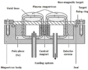
Fig.3.8 Principle of the magnetron device
3.3.3. Physical mechanism of a thin layer
formation
The formation of thin layers by physical vapor deposition is
the result of the condensation of the particles ejected from the target onto
the substrate. It is carried out by a combination of nucleation and growth
processes described in Figure 3.9.
At the moment of impact on the substrate, the incident atoms
lose their kinetic energies and produce the limiting of their ability to
diffuse into the substrate. This is true only if there is no external energy
supplied to these particles by heating the substrate or ion bombardment. Since
they are first adsorbed, they are known as adatoms. Those
adatoms move on the surface until the thermal equilibrium with the substrate is
reached.
During their displacement, the adatoms interact with one
another; creating nucleus called clusters which continue their
displacement by developing and colliding with each other. The clusters continue
to grow in number and size until a nucleation density known as saturation
density is reached.
The next step in the process of forming the thin layer is
called coalescence. The clusters begin to agglomerate with each other by
reducing the surface area of the uncoated substrate. The coalescence can be
accelerated by increasing the mobility of the adsorbed species, for example by
increasing the temperature of the substrate. During this step, new clusters may
be formed on surfaces released by the approach of older clusters. The clusters
continue to grow, leaving only holes or channels of small dimensions between
them. Gradually, a continuous layer forms when the holes and channels are
filled.
44
Chapter 3: Vapor deposition and thin layer
characterization techniques
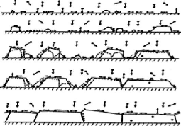
Fig.3.9 Layer growth process: nucleation and clusters
growth
There are three modes of clusters nucleation and growth:
- A cluster called Volmer-Weber (fig.3.10. (a)):
During three-dimensional growth, or Volmer-Weber growth, clusters
form and their coalescence forms a film. This mode of growth is usually favored
when the atoms forming the deposited layer are more strongly bonded to one
another than to the substrate.
- A cluster called Frank-Van der Merwe (fig.3.10 (b)):
The Two-dimensional (2D) growth, or Frank-Van der Merwe growth,
is favored when the binding energy between the deposited atoms is less than or
equal to that between the thin layer and the substrate. So, the films form
atomic layer by atomic layer.
- The mixed type called Stranski-Krastanov (fig.3.10. (c)):
The third mode of growth, called Stranski-Krastanov, is a
combination of the two preceding modes: after two-dimensional growth begins, a
change in growth mode is observed, while clusters formation becomes
energetically favorable.
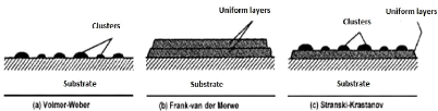
Fig.3.10 Main growth modes of thin films
3.3.4. Thin film morphology
The growth mode of layers as well as the deposition conditions
(substrate temperature, substrate nature, partial gas characteristics, etc.)
influence on the crystallographic orientations and the topographical details of
the clusters.
In fact, several models based on thin film growth approaches
have been developed to study the influence of the deposition parameters on the
microstructure of the layers. The first
45
Chapter 3: Vapor deposition and thin layer
characterization techniques
description of the morphology of thin layers obtained by
physical vapor deposition was presented by Movchan and Demchishin (fig.3.11)
[MOV69]:
- First zone: the working pressure is greater than or equal to
1 mbar and the deposition temperatures are between 0.1 and 0.2 times the
melting temperature of the deposited metal, this zone is favorable for
applications or wettability of the surface is sought but not suitable for
corrosion resistance or mechanical strength.
- Second zone: is called also the transition zone where the
crystallization of the deposit is very fine with good properties in terms of
resistance to corrosion and adhesion.
- Third zone: where the columnar crystallization is well
identified, this zone is preferred for mechanical applications because of the
good adhesion properties obtained.
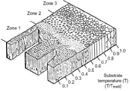
Fig.3.11 Movchan and Demchishin structural model
Thornton [THO77] proposes a model that complements the
previous one by considering the argon pressure in the sputtering. Its model
shows a transition zone, called zone T, between zones 1 and 2 (fig.3.12). In
this zone, the grains have a fibrous form without microporosities.
Later, Messier [MES84] showed that the fundamental process
controlling the morphology of the T-zone was not only the gas pressure but also
the effect of the gas pressure on the ionic bombardment of the growing film
surface during the deposition by cathodic sputtering. He proposed a fifth zone
M of morphology consisting of parallel columns with a domed surface
(fig.3.13).
Chapter 3: Vapor deposition and thin layer
characterization techniques
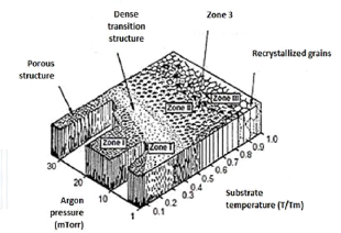
Fig.3.12 Structural modal of Thornton
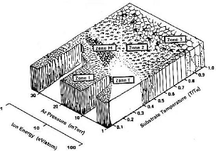
Fig.3.13 Structural modal of Messier
46
3.4. Methods of microstructural
characterization
After the application of the layer on the sample, this layer
must be characterized. First, we must study its morphology using chemical,
crystallographic and microstructural techniques (Table 3.5), and then we
characterize one or more properties of this deposit (mechanical, optical,
electrical, chemical properties, etc.). These properties are generally studied
with all
47
Chapter 3: Vapor deposition and thin layer
characterization techniques
results of morphological studies, in order to draw a
conclusion either to modify the deposition process or to apply it in
industry.
The greatest difficulty in the characterization phase is that
these techniques are indirect. So, the engineer's art consists in crossing the
results obtained, to constitute a global and synthetic vision of the most
realistic product possible, in order to be able to produce a list of functional
characteristics.
|
Chemical characterization
methods
|
Crystallographic
characterization
methods
|
Microstructural
characterization methods
|
|
- Auger Electrons Spectroscopy
|
|
|
|
(AES)
|
|
- Atomic force microscope
|
|
- Energy Dispersion Microscopy
|
|
(AFM)
|
|
(EDS)
|
|
- Scanning Tunnel microscope
|
|
- Electron Energy Loss
|
- Selected area diffraction
|
(STM)
|
|
Spectroscopy (EELS)
|
(SAD)
|
- Optical Microscope (LM)
|
|
- - Electronic microprobe analysis
|
- X-ray diffraction (XRD)
|
- Scanning electron
|
|
(EMPA)
|
|
microscope (SEM)
|
|
- Raman Spectroscopy (RS)
|
|
- Transmission electron
|
|
- X-Ray Photoelectron spectroscopy
|
|
microscope (TEM)
|
|
(XPS)
|
|
|
Table 3.5 the classification of main morphological
characterization techniques of a thin layer
3.4.1. Chemical characterization methods 3.4.1.1.
Auger Electrons Spectroscopy (AES)
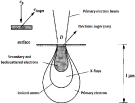
Fig.3.14 Distribution of the primary, Auger and backscattered
electrons, as well as X-rays under bombardment of a focused primary electron
beam of a diameter D
48
Chapter 3: Vapor deposition and thin layer
characterization techniques
This technique consists in bombarding the layer with an
energetic primary electrons (3 to 30 KeV), which penetrates into the matter at
depths of the order of some micrometers and excites the atoms of the layer, the
de-excitation can be carried out by emission of the secondary electrons, and of
the Auger electrons after the relaxation.
These electrons are characteristic for each atom, and the
study of their spectrum makes it possible to identify the chemical composition
of the deposit, the atlas of the spectrums of the Auger rays is available in
the literatures.
The AES technique is used to analyze the most superficial
atomic layers for conductive and semiconductive samples.
3.4.1.2. Energy Dispersion Microscopy
(EDS)
This technique involves bombarding the layer by a beam of
primary electrons; this beam can cause the emission of X-rays. The emitted
spectrum breaks down into two radiations: a continuous radiation and a
characteristic radiation which created after an inelastic impact between the
atom and the electron. The characteristic radiation is specific for each
element, and its detection allows for chemical analysis.
3.4.1.3. Electron Energy Loss Spectroscopy
(EELS)
This technique involves exposing sample to a primary electron
beam; some of these electrons will be subjected to inelastic impacts with the
atoms of the sample, which causes the loss of their energy and a weak or random
deflection of their trajectory. This loss of energy can be measured, and the
spectrum can be used to determine the chemical characteristics of the
sample.
3.4.1.4. Electron microprobe analysis
(EMPA)
This technique is based on the analysis of the X-rays emitted
by the atoms of the sample after inelastic impacts with the electron beam. The
X-radiation is sent to a monochromator which is a single crystal having
well-known crystalline planes. This radiation is then diffracted, and the
diffraction angle varies as a function of the wavelength.
3.4.1.5. Raman spectroscopy (RS)
The Raman effect results from the slight change in the
frequency of the monochromatic light projected on the sample, this modification
is caused by the vibrations and / or the rotations of the molecules. The
spectrum analysis of the scattered light gives information on the molecular
composition of the sample, because the spectrums of the vibrations are
characteristic for each molecule.
3.4.1.6. X-Ray Photoelectron spectroscopy
(XPS)
Also called ESCA (Electron Spectroscopy for Chemical
Analysis), this technique involves bombarding the sample with X-rays; the
photons y of these rays enter the sample and ionize
the atoms. The photons have kinetic energies E??
which correspond to the ionization energies E
of the different orbits of the atom by the relation:
49
Chapter 3: Vapor deposition and thin layer
characterization techniques
E = h?? - E?? (3.18)
h: Is Planck constant;
The energy of the electrons in each orbit is specific for each
atom, so the knowledge of the energy of the projected photons h??
and the analysis of the kinetic energy of the photons makes it
possible to identify the chemical composition of the sample. The average
analysis depth by this technique is from 1 to 5 nm.
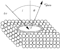
Fig.3.15 Principle of XPS analysis
3.4.2. Crystallographic characterization
techniques
Crystallographic analysis techniques are based on the
principle of X-ray diffraction (XRD) or electron-associated wave (SAD). These
techniques make it possible to determine:
- Crystalline phase composition;
- The orientation and degree of organization of the crystal
grains;
- Stress inside the repository.
3.4.2.1. Selected area diffraction
(SAD)
A primary beam of electrons passes through a thin sheet; the
wave associated with the electrons is submitted to diffraction on the
crystalline planes of the sample. The transmission electron microscope TEM
allows obtaining the image and the spectrum of this diffraction. The SAD
technique makes it possible to obtain the information for very small
crystalline grains.
3.4.2.2. X-ray diffraction (XRD)
The X-rays are diffracted on a crystalline plane according to
Bragg's law: A = 2d sin?? (3.19)
The diffracted X-Rays wavelengths vary between ë = 0.071
nm (source with molybdenum anode) and ë = 0.154 nm (source with copper
anode).
Chapter 3: Vapor deposition and thin layer
characterization techniques
The diffraction experiments are done differently for thick
layers (more than 10 ìm) and for thin layers. The thick layers are
tested with a diffractometer in which the radiation source and the detector
move circumferentially around a sample, placed at its center, the radiation
penetrates into the interior of the layer and the signal of the substrate is
low. This technique should not be applied to thin films because the signal of
the substrate would be dominant compared to that of the deposit. In this case,
the surface diffraction technique (GRXD) in which the incident beam interacts
with the surface of the layer at a small angle varying from 1 to 10 ° so
that to have a penetration depth of less than 1 ìm, the detector moves
to obtain the diffracted signal.
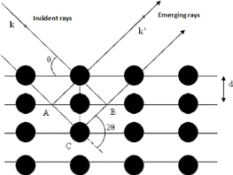
Fig.3.16 Bragg law principle
3.4.3. Microstructural characterization
methods
The microstructure analysis concerns the study of the layer
surface (AFM, STM) as well as the study of grains inside the deposit (LM) or
the internal grain morphology (TEM).
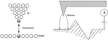
3.4.3.1. Scanning Tunnel microscope
(STM)
The STM is used to characterize the surface of conductive or
semiconductive materials. This microscope has a tip whose end has the size of
an atom.
50
Fig.3.17 operating principle of the STM
Chapter 3: Vapor deposition and thin layer
characterization techniques
The principle (figure 3.17), is to set a distance less than 1
nm (interatomic distance) between this tip and the surface of the sample, which
allows the exchange of electrons and cause an electrical voltage of U = 2mV to
2V, the resulting current is called the tunnel electron current. Since this
current is very sensitive to any changing in the distance between the tip and
the surface, so this distance must be kept constant. This principle allows
obtaining a map with a very good vertical resolution of the surface.
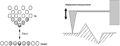
3.4.3.2. Atomic force microscope
(AFM)
Unlike the STM, the AFM was developed to obtain surface
profiles of non-conducting materials. The tip of the probe is equipped with a
small diamond that touches the surface of the layer with a small force varying
between F = 10-6 and 10-9 N to avoid any damage to it.
The diamond is attached to a lever of which while the displacement occurs, the
measurements are made by very sensitive sensors (fig.3.18).
51
Fig.3.18 Operating principle of the AFM 3.4.3.3.
Optical or Light microscope (LM)
The use of the optical microscope requires special preparation
of the layer surface. This microscope allows observing the porosity and the
distribution of the pore size, the size of the unfused particles and their
distributions, the thermal and mechanical deformation of the substrate at the
interface with the deposit, the phase distribution in a composite deposit, etc.
. .
3.4.3.4. Scanning electron microscope
(SEM)
The operating principle of the SEM is the projection of a
primary electron beam which scans the sample surface and which accelerates by a
voltage of U = 1 to 30 kV. The beam of electrons interact with the atoms of the
sample either by inelastic impacts followed by their ionization and by the
generation of secondary electrons with a kinetic energy of E?? < 50 eV
coming from the superficial region of the deposit (some nanometers), or By
elastic impacts with these
52
Chapter 3: Vapor deposition and thin layer
characterization techniques
atoms and the generation of backscattered electrons with a
kinetic energy of E?? > 50 eV coming from the deeper regions
(hundreds of nanometers).
The secondary electrons are detected by a scintillation
detector equipped with a grid carried at the positive potential to attract
these electrons at low energy. The backscattered electrons are detected by a
semiconductor detector.
3.4.3.5. Transmission electron microscope
(TEM)
The operating principle of this microscope is the emission of
a beam of primary electrons passing through the sample. The image in this
microscope is obtained by electrons that have not interacted with the sample.
The electrons are accelerated by a voltage of several hundreds of kV to be able
to cross slides, which must have a thickness less than 100 to 200 nm.
3.4.4. Mechanical characterization 3.4.4.1.
Hardness
Three types of hardness are defined depending on the depth of
indentation (Table 3.6). The loads used depend on the type of hardness. In
nanohardness these charges range from some micronewtons to several hundredths
of millinewtons, while microhardness requires loads ranging from a few tens of
millinewtons to a few Newtons, in macrohardness the loads range from a few
Newtons to several tens of Newtons.
|
nanohardness
|
microhardness
|
macrohardness
|
|
Depth of indentation (rim )
|
0.001 - 1
|
1 - 50
|
50 - 1000
|
Table 3.6 Types of hardness
The use of each type of hardness depends on the material being
tested, so the nanohardness is used to characterize thin layers with
thicknesses of less than one micrometer, whereas the microhardness used to
study certain surface treatments such as shot blasting or Thermo-chemical
treatments (carburizing, nitriding, etc.). The macro hardness is used to
measure the hardness of the steels after a heat treatment for example.
With the appearance of nanohardness since 1990, it was
possible to understand different mechanical characteristics of materials at the
sub-micron scale. However, although this test is fairly simple to carry out in
principle, its technological implementation remains delicate, and the
interpretation of the results is not simple. Indeed, it is a test, although
extremely powerful, which requires a particular attention during the testing,
and the analysis of the information.
The nanohardness test consists in the simultaneous measurement
of the force F applied to the indenter and of its
penetration h into the material under investigation. The representation
F = f (h) for the charge and the discharge
constitutes the nanoindentation curve.
The inverse analysis by finite elements analysis of the
indentation curves allows, to some extent, to have mechanical properties such
as: modulus of elasticity, hardness tensile strength, etc.
53
Chapter 3: Vapor deposition and thin layer
characterization techniques
The interpretation of the measured characteristics (and in
particular the hardness) by the nanoindentation test requires simultaneous
consideration of the ISE (Indentation Size Effect) and the exact shape of the
indenter tip (Berkovich or Vickers), and without forgetting the effects of
roughness.
We can observe hardness variations of the order of few
percents due to the presence of internal stresses in the materials tested, this
is particularly true for thin films.
3.4.4.2. Adhesion of coatings
It is assumed that the adhesion of protective film is an
indispensable condition, because of that, the deposition of a coating film is
always preceded by a mechanical and / or chemical treatment intended to clean
and activate it in order to optimize the adhesion of the film to the substrate.
It is also often the practice to deposit an intermediate film (bonding layer)
between the substrate and the final coating, for example, a layer of silicon is
deposited on steels before being coated with a DLC layer.
For the characterization there are two main families of
techniques: non-destructive and destructive techniques. The first uses an
optical or acoustic probe that explores the coated material and detects any
defect or inhomogeneity (cracks, porosities, bubble etc.) at the film-substrate
interface. The most used amongst these methods are the ultrasonic methods.
Destructive techniques can be divided into two categories:
- Techniques used for ductile or weakly adherent coatings
(paints, varnishes, polymers, etc.): like the peeling test, the swelling
test...
- Techniques for metallic or ceramic coatings or when the
adhesion is strong: as the scratch test.
- Peeling test
This test consists in applying a force F, at an angle
è, to a band of length b, deposited on a substrate (Figure. 3.19). This
force increases gradually over time until the force F??
corresponds to the initiation of the flow of the film. The operation
is then continued at constant speed until the complete flow. At the end of the
test, it is necessary to check the condition of the uncoated strip and that of
the substrate in order to check that there is no elongation or plastic
deformation and that all the energy expended during the flow of the band
interface was used to break the bonds at the substrate-band interface.
The rate of release energy is given by:
G = (F??? ?) (1 - ????????) [??m-2]
(3.20)
Chapter 3: Vapor deposition and thin layer
characterization techniques
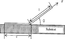
Fig.3.19 principle of the peeling test
54
- Blister Test:
This test consists in making an opening in the substrate in
such a way to retain the initial thickness of the film. A pressure P on the
deforming film is then applied using an incompressible fluid. The film will
begin to swell progressively up to a certain critical height ????
corresponding to a pressure P?? and then begin to peel
off from the substrate (Fig.3.20).
The rate of return of energy is given by:
G = ??P?????? (3.21)
?? : Constant having a value between 0.5 and 0.65;
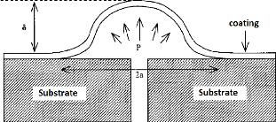
Fig.3.20: Principle of the Blister Test
- Scratch Test
This test consists in applying, perpendicularly to the surface
to be tested, a sharp Rockwell-type indenter (cone with an angle of 120 °
and a radius of curvature of 200 ìm) supporting a load of between 1 and
200 N which increases linearly over time with a loading rate of 10?? ·
m????-1. When the indenter sinks into the surface of the
material, it is made to slide with a velocity of 10 mm.
m????-1 (fig.3.21).
55
Chapter 3: Vapor deposition and thin layer
characterization techniques
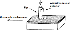
Fig.3.21 Principle of Scratch Test
3.4.4.3. Residual stresses in the
coatings
In the production of a high-temperature coating ( PVD or CVD),
at the time of return to ambient temperature, due to the difference in the
coefficient of thermal expansion between the coating and the substrate,
internal stresses can appear in the film, and the deposition-substrate assembly
can deform if the substrate is sufficiently thin (some tens to a few hundreds
of micrometers thick), in this case the direction of convex or concave
deformation indicates, whether they are tensile or compressive stresses .
The internal stresses have an important role because they can
influence both the hardness of the coating, its adhesion to the substrate and
also its resistance to wear and cracking.
The two main techniques used for the determination of internal
stresses are X-ray diffraction and the Stoney method. The two methods consist
in reducing the thickness of the substrate by machining to such a value in
which the action of the residual stresses is manifested.
- The Stoney method (the determination of the
internal stresses by measuring the radius of curvature):
From this technique, the mean internal stresses ó can be
calculated using the expression:
h?? 2????
?? = ????h??(1 - ????) (3.22)
h??, ????, ????: Are the thickness, the Young's modulus and the
Poisson's ratio of the substrate;
h??: The coating thickness; ??: The radius of curvature.
This relation makes sense only when the ratio (h??/h??) is of the
order 5 to10 % .
3.5. Thin films deposits properties
PVD and PACVD thin films are used to improve friction and wear
resistance. Table 3.7 gives the main mechanical and tribological
characteristics of the layers produced:
56
Chapter 3: Vapor deposition and thin layer
characterization techniques
|
coating
|
TiN
|
(Ti,Al)N
|
TiCN
|
CrN
|
DLC
|
|
Color
|
Yellow gold
|
black
|
purple
|
silver
|
back
|
|
Hardness (HV)
|
2300 à 2500
|
2500 à 3200
|
3000 à 3400
|
1800 à 2200
|
3500 à 5000
|
|
oxidation résistance (°C)
|
400
|
800
|
300
|
600
|
400
|
|
Elaborating temperature (°C)
|
250 à 400
|
450
|
450
|
600
|
200 à 400
|
|
thickness (um)
|
2 à 5
|
2 à 5
|
2 à 6
|
3 à 8
|
1 à 4
|
|
Dry friction on 102 Cr6
|
0.55 à 0.65
|
0.50 à 0.60
|
0.45
|
0.40 à 0.55
|
0.05 à 0.07
|
- The coating of (Ti,Al)N is the most resistant to oxidation, so
it will be used under severe thermal conditions.
- The DLC coating is the one which have the best tribological
characteristics because of the presence in its microstructure of a large
proportion of graphite bonds; it is therefore used for delicate lubrication
conditions.
- The TiCN coating has a good hardness property, with good
conductivity; it will therefore be used with strong mechanical stresses such as
steels.
- The CrN coating has good ductility and good resistance to
oxidation.
Chapter 4
Experimental Process
54
Chapter 4: Experimental Process
4.1. Determination of the sample grade
The piston used in our study as a substrate is HATZ E780. The
materials used to make this piston are: Cast iron and aluminium-silicon
eutectic alloy, the main production processes are: melding, forging
[GER/https].
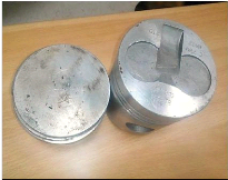
Fig.4.1: The piston HATZ E780 studied
According to the XRD analysis it can be ensured that the material
used for piston manufacture is the eutectic Al-Si alloy fig. 4.2.
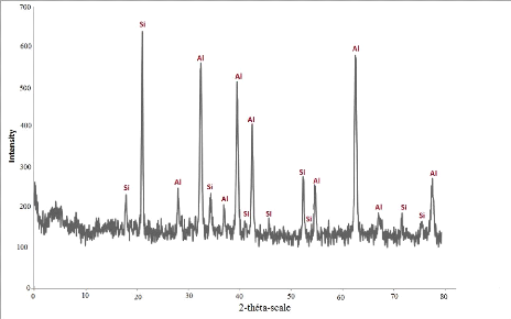
Fig.4.2: XRD spectra of a sample of the piston HATZ
E780
55
Chapter 4: Experimental Process
The silicon content in aluminium for a eutectic Al-Si alloy is
varied between 11.7 % and 14.5 % the average
value is generally 12.5%. The most commonly used eutectic
alloys for the manufacture of pistons are given in table 4.1
[EUR/http]:
|
Continent
|
4032 (AW-AlSi12,5MgCuNi)
|
4047A (AW-AlSi12 (A))
|
4045 (AW-AlSi10)
|
|
Si %
|
11-13.5
|
11.0-13.0
|
9.0-11.0
|
|
Fe %
|
1.0
|
0.6
|
0.8
|
|
Cu %
|
0.8-1.3
|
0.3
|
0.3
|
|
Mn %
|
|
0.15
|
0.06
|
|
Mg %
|
0.8-1.3
|
0.1
|
0.05
|
|
Zn %
|
0.25
|
0.2
|
0.1
|
|
Ti %
|
|
0.15
|
0.2
|
|
others %
|
0.2
|
0.2
|
0.2
|
|
Al %
|
Rest
|
Rest
|
Rest
|
Table 4.1: most commonly used eutectic alloys for the
manufacture of pistons
4.2. Preparation of samples
4.2.1. Samples Cutting
The piston with cylindrical shape is cut in the workshop in order
to obtain samples with dimension of (20×10×6) mm; the cutting
operation is divided into two stages:
First stage: Consists of piston separation in
two sections (Head and skirt) By means of a metal chainsaw
Second stage: Consists in cutting the upper part
of the piston obtained by the preceding method with the aid of a hacksaw into
samples of well-defined size.
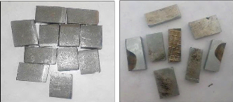
Fig.4.3: cutting samples, on the left stainless steel, on
the right aluminium
56
Chapter 4: Experimental Process
4.2.2. Samples polishing
In the process of surface preparation operations, polishing is
essentially a finishing operation, the purpose of which is to:
- reduce roughness and surface topology by eliminating surface
defects such as microcracks, porosities and inclusions.
Using a MECAPOL 230 polisher (fig.4.4), The 304 stainless steel
substrates and the Al-Si substrate are polished, using abrasive papers with
particles size varied from (200 to 1200) it is a kind of sandpaper, but with a
larger particle size Fine and controlled.
Obtaining of the polished surface finish is done progressively
(from the big size to the small one) in the presences of the water for the
cooling and the evacuation of the debris.
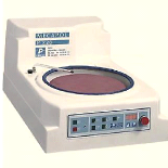
Fig.4.4 : MECAPOL 230 polisher
Characteristics of the device
- The polishing head makes it possible to process up to 6 samples
Ø 50 mm flanged in a plate by central pressure.
- Pressure force between 0.5 à 30 daN.
- Time between 10s to 99 minutes.
- Rotating speed between 20 à 600 rpm/mn.
4.2.3. Chemical cleaning
The purpose of chemical cleaning is to remove contamination or
impurities formed after polishing to ensure good adhesion of the deposit.
The samples are immersed in an acetone bath for about 5
minutes; then rinsed with distilled water and then dried with the aid of
compressed air.
4.3. Thin film elaboration process
In our work, we will deposit a thin layer on three types of
samples with different substrates in
order to better characterize the layer obtained:
- Four samples of a substrate obtained from an Al-Si alloy piston
HATZ E780;
- Four samples of 304 stainless steel substrate;
- Five samples of a 304 stainless steel substrate on which an
Al-Si layer is deposited;
57
Chapter 4: Experimental Process
- In four of the previous five samples, a layer of Ti-W-N is
deposited.
We use the PVD sputtering technique to deposit thin layers of
Ti-W-N on Al-Si, stainless steel 304 and stainless steel with intermediate
layer of Al-Si, the evaporation technique was used to create the intermediate
layer
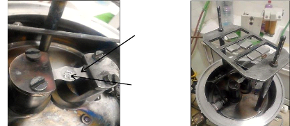
4.3.1. Description of PVD sputtering installation and
working parameters
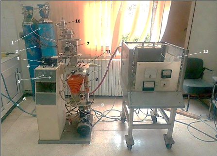
Fig.4.5. PVD sputtering installation of the CDTA
1) Bottle of nitrogen gas - 2) Nitrogen passage line - 3)
Primary pressure gauge - 4) secondary pressure gauge - 5) Primary and secondary
pump ignition switches - 6) Secondary Pump Cooling Water Pipe - 7) deposition
reactor - 8) Secondary diffusion pump - 9) Pallet primary pump - 10) Gas
pressure control valve (nitrogen and argon) - 11) Throttle valve - 12) Power
supplies
The deposition chamber is cylindrical in shape, with a high of
230 mm, diameter of 210 mm, the interelectrode distance is 45 mm, and the lower
part of the chamber is connected to the pumping system.
The primary pump is an Alcatel-type pump that can achieves a
vacuum of up to2 · 10-2???????? (2.67 ·
10-2????????) And a flow rate of0.5 à 70
????3 /?? .
The secondary diffusion pump used allows a vacuum to reach
10-5???????? (1.33 · 10-5????????) And a
flow rate of 250 ????3 /?? .
Chapter 4: Experimental Process
The primary pressure gauge is Priani type, it measures pressures
up to 10-3Torr (1.33 · 10-3 mbar). The secondary
pressure gauge is a Penning type gauge, the measured pressure can
reach10-5Torr (1.33 · 10-5 mbar).
The power generator supplies the system with a maximum electrical
power of 20 Watt, a voltage of 2 kV and an electrical current of 10 mA.
The working parameters are:
- The application of argon alone for 5 minutes with a pressure of
9.5 · 10-2Torr ; (0.127 mbar). Argon ions spray directly the
target, allowing surface cleaning;
- The introduction of nitrogen into the plasma for one hour with
the pressure of 0.1 Torr (0.133 mbar);
- The percentage of nitrogen introduced into the plasma is 5%
;
- The working voltage is 2 kV.
|
a)
|
|
b)
|
|
|
Fig.4.6: the deposits obtained on the PVD sputtering
installation:
- a) on Al-Si,
- b) on stainless steel,
- c) on stainless steel with
intermediate layer of Al-Si
|
c)
|
b)
|
58
4.3.2. Description of PVD evaporation installation
and working parameters
The working parameters are:
- The limiting pressure of the primary pallet pump is 10-2
mbar ;
- The limiting pressure of the secondary diffusion pump is 3
· 10-5 mbar ;
- in order To have a thin layer on stainless steel similar to
aluminium-silicon eutectic alloy (of 12.5 % Of silicon content see chapter 2),
il faut Put on the crucible 60 mg of powder contains 52.5 mg of the aluminium
powder and 7.5 mg of the silicon powder.
59
Chapter 4: Experimental Process
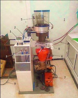
Fig.4.7: The PVD by evaporation installation of
CDTA
1) Primary pressure gauge - 2) Secondary pressure gauge - 3)
Primary and secondary pump ignition switches - 4) Secondary Pump Cooling Water
Pipe - 5) Deposition reactor - 6) Secondary diffusion pump - 7) Pallet primary
pump - 8) Throttle valve - 9) To power supply
a)
b)
The crucible of the evaporator
Al-Si powder To evaporate
Fig.4.8: Inside the reactor chamber: a) Al-Si powder on the
crucible, b) The samples of stainless
steel on the substrate port
60
Chapter 4: Experimental Process
4.4. X-ray diffraction
An indispensable complement to elemental chemical analysis for
the identification of compounds, X-ray diffraction allows the fine
characterization of massive crystallized materials
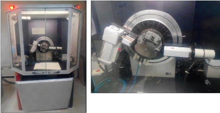
Fig.4.10: Our sample at the interior of the
diffractometer
Fig.4.9: Diffractometer D8 ADVANCE of CDTA
4.4.1. Characteristics of the device
· The diffractometer uses the BRAGG-BRENTANO assembly;
· Source (anticathode) of copper;
· Point scintillation detector;
· Acquisition range between 0 ° and 90 °. With
precision of steps up to 0.01°;
· Grazing incidence configuration, with a minimum angle of
incidence of 0.1 °;
· Eva operating software.
4.4.2. Working Principle [CDTA/http]
X-ray diffraction gives access to many information contained
in the arrangement of atoms within a crystallized material and The 3D
geometrical type of arrangement (network), the distances between atoms (mesh
size, typically a few Å) which constitute schematically a "unique"
identity card for each compound.
The BRUKER D8 Advance diffractometer is equipped with a
BRAGG-BENTANO geometry goniometer. In this type of diffractometer, an incident
monochromatic X-ray beam is diffracted by the sample at certain specific
angles, According to Bragg's law: 2dhkl
sinè = A, in which dhkl Refers to the
interreticular distance of family plans (hkl), è Is the angle of
incidence taken from the surface of the planes (hkl) ,ë The wavelength of
the scattered photons.
61
Chapter 4: Experimental Process
As Lambda does not vary during a measurement, it is enough to
vary the angle Theta to locate all diffraction angles. By means of a converter
- a scintillation counter, the intensity of each point of the measurement is
thus observed.
When the X-ray beam is diffracted, its representation is a
peak. A Theta scan produces an X-ray diffraction pattern.
The recording of the signal by a suitable detector makes it
possible to visualize the angles and Intensities of the diffraction peaks
obtained. The indexing of these peaks is carried out using specific databases
that have more than 350 000 records. Allowing the identification of the
compound (s).
4.5. Raman Spectroscopy
4.5.1. Principle of RAMAN spectroscopy
During the interaction of a light beam with the material,
several phenomena can occur. A part of the light beam is reflected, a part is
diffused and a part can be transmitted through the sample (figure 4.11). During
propagation in a dense medium, different phenomena appear: refraction,
absorption, diffusion, and possibly other non-linear effects. The absorption
may then induce photoluminescence or non-radiative de-excitation processes.
The scattering of light is manifested by the deflection of a
part of the light beam in multiple directions. The majority of the scattered
light is of the same energy as the incident light. This phenomenon of elastic
diffusion is called Rayleigh scattering. However, a small portion of the
scattered light (about one photon out of 106) present gain or loss of energy
relative to the incident light. This is the phenomenon of Raman scattering. In
a classical approach, this phenomenon of inelastic diffusion is explained by
the creation of an induced dipole which oscillates at a frequency different
from that of the incident light. Indeed, under the action of a monochromatic
electromagnetic wave of frequency ù whose electric field oscillates
according to:
??= ??0 cos(????) (4.1)
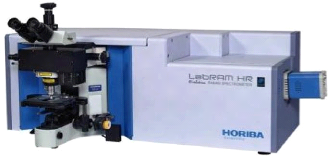
Fig.4.11: Spectrometer Raman HORIBA of CDTA
62
Chapter 4: Experimental Process
The Stokes diffusion and the anti-Stokes diffusion would be of
the same intensity. However, experimentally the intensity of the Stokes
diffusion is always (outside resonance) higher than that of the anti-Stokes
diffusion.
4.5.2. The information accessible by Raman
spectrometry
The information provided by Raman spectroscopy is relatively
extensive:
- Identification of phases or chemical compounds ·
- Characterization of materials ·
- Determination of the molecular structure ·
- Study of amorphous and crystalline systems.
The Raman spectrum of a compound indicates both the type of
binding of a compound and its crystalline structure.
4.6. Scanning electronic microscope (SEM)
The scanning electron microscope provides surface images of
virtually all solid materials at scales ranging from the magnifying glass (x10)
to that of the transmission electron microscope (x 500,000 or more).
Conventional SEM operates in an ordinary vacuum (10-5 to 10-6
mbar); The samples may be massive, ranging in size from a few ìm
(particles) to about tens of cm in diameter, or even more (industrial samples).
They must endure the vacuum. The preparation is generally simple.
The SEM at low pressure allows observation in a vacuum of up
to 30 mbar, making it possible
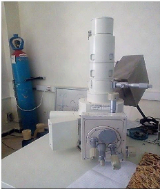
fig.4.12: scanning Electronique microscope JEOL JSM 6360LV de
CDTA
Chapter 4: Experimental Process
to examine moist or oily samples, insulators without prior
metallization (ceramics, corroded metals).
Characteristics of the device
? A maximum resolution of 50 nm.
? The SEM is coupled to the EDS for the elementary
microanalysis.
? Maximum voltage 30 kV.
4.7. The nanoindentation
Fig.4.13: The nanoindentation device CSM_NHT of CDTA
The indenter used on our characterization equipment CSM_NHT
(Nano-Hardness Testers is a Berkovich indenter (pyramidal with triangular base
geometry). We can apply a normal force between 0.3mN and 500mN.
|
h
cos65.27° = b
a = 2v3 h ??a??65.3°
|
|
63
Fig.4.14: The geometry of Berkovich Point
Chapter 4: Experimental Process
64
Fig.4.15: the footprint of the Berkovich tip
During an indentation test an acquisition system records the
applied force as a function of the penetration depth of the tip. These two
parameters are measured during a charge phase and a discharge phase. The result
is a load-displacement curve.
The two main properties measured by the nanoindentation are
the modulus of elasticity (E) and the hardness (H). The model used for the
calculation of these two properties is that developed by Oliver and Pharr.
According to this model the hardness is given either geometrically (fig.4.16)
or analytically by:
????????
H = (4.2)
????
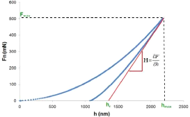
Fig.4.16: The determination of the hardness from the
charge-discharge curve
Fmax : Maximum applied load;
Ac : The contact area between the indenter and the
sample which is given in the case of a Berkovich indenter by:
65
Chapter 4: Experimental Process
A?? = 24,56 · hC 2 (4.3)
????????
hC= h?????? - ??· (4.4)
??
???? 2
?? = ??h = · ???? · vAC (4.5)
vit
Er : reduced Modulus of elasticity.
The modulus of elasticity of material is given by:
?? = (1 - v2) ( ???? · ???? )
(4.6)
????(1 - v??2) - ????
ui: Poisson's ratio of the indenter; u:
Material Poisson's ratio;
Ei : Modulus of elasticity of the indenter.
In our nanoindentation tests, we used the Oliver-Pharr model with
the following parameters:
- Spherical diamante Berkovich indenter ( r =
10ìm) in diameter
- approaching speed: 2500 nm/min
- Time of charge and discharge: 10.0 s
- Linear load increment
- Slope to contact: 80%
- Load Speed: 2.00 mN/min
- Speed of discharge: 2.00 mN/min
- Material Poisson's ratio u = 0.30
This device is equipped with an optical microscope to select the
area to be indented. An X-Y
motorized table with a repositioning accuracy of 1 ìm
allows the programming of complex
indentation networks.
4.8. The tribometer analysis
On the CSM tribometer (fig.4.18), a ball, a tip or a plane is
placed in contact with the surface of the sample under a predetermined load.
The device is mounted on a lever arm, and associated with a displacement
sensor.
The coefficient of friction is determined during the test by
measuring the deflection of this elastic arm. The wear rates for the ball and
the pawn are calculated by determining the loss of volume during the test. The
formula for determining the wear rate WS is given by:
??
????= ?? · ???? (4.7)
66
Chapter 4: Experimental Process
??: The volume of lost matter
(mm3) ;
D: The covered distance (mm)
;
F??: The normal force applied to the sample
(N).
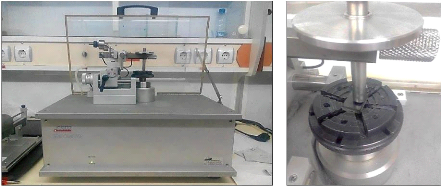
fig.4.17 : Tribometer of the USTHB
The volume of the waste material is calculated by the
formula:
?? = 2??R [r2 aresi?? (d2r) -
(4d) · v4r2 - d2] (4.8)
R: Radius of the wear track
(mm);
r: Radius of the ball (mm);
d: Width of the wear track
(mm).
Tribometer analysis facilitates the study of friction
mechanisms for a wide variety of material couple with or without lubricating
agent. In addition, the control of test parameters such as speed, contact
pressure, frequency, test duration and environmental parameters make it
possible to reproduce the actual stresses of use of these
materials.
Instruments can provide rotational or alternative
movement of the sample. A particular point of these instruments is based on the
possibility of interrupting the test as soon as the coefficient of friction
reaches a predefined value or, when a number of cycles is realized. In
addition, the tribometer is equipped with a containment enclosure in order to
use the instrument under controlled atmospheric temperature
conditions.
The Tests performed by tribometer conforming to ASTM G99
& DIN 50324.
The specifications of the CSM tribometer are:
67
Chapter 4: Experimental Process
|
Nano
|
Micro
|
|
Normal Strength Range
|
50 ìN - 1 N
|
until 60 N
|
|
Maximum tangential force
|
10 ìN - 1 N
|
10 N
|
|
Maximum temperature
|
-
|
1000 oC
|
|
Rotation speed
|
1 - 100 rpm
|
0.3 - 500 rpm
|
|
Rotating test radius
|
30 ìm - 10 mm
|
30 mm
|
|
Linear travel speed
|
10 - 500 ìm
|
60 mm
|
|
Length of linear travel
|
Until 10 mm/s
|
until 100 mm/s
|
|
Frequency
|
0.1 - 10 Hz
|
1.6 Hz
|
|
Penetration depth measurement
|
20 nm - 50 ìm
|
until 1.2 nm
|
Table 4.2: The specifications of the CSM tribometers
The characteristics of our work:
- Geometry of the tip: Ball;
- Material of the tip: alumina????2??3 ;
- Radius of the ball: 3.00 mm;
- Linear speed: 0.50 cm/s;
- Normal load: 1.00 N;
- Stop condition: 10.00 Meters travelled or if ii > 1.00 ;
- Temperature: 20.00 °C ;
- Humidity: 40.00 %.
4.9. Electrochemical techniques
4.9.1. Equipment
The polarization measurements were carried out in a
three-electrode glass cell: a working electrode, a platinum counter electrode
and a saturated calomel reference electrode (SCE). This cell, shown in figure
4.18, is designed to maintain a fixed distance between the three electrodes.
The passage of the current in the cell is carried out through the
counter-electrode.
68
Chapter 4: Experimental Process
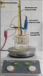
Figure 4.18: the Cell used in electrochemical test
Electrochemical measurements were conducted using a
computer-controlled, potentiostat, model parstat 4000 (Fig.4.19).
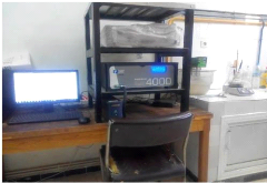
Fig.4.19: Assembly for electrochemical testing
4.9.2. Establishment of EVANS diagrams
The purpose of the EVANS diagram is to rapidly obtain, by a
laboratory measurement, the corrosion rate and the corrosion current density
denoted icorr from the polarization curves
69
Chapter 4: Experimental Process
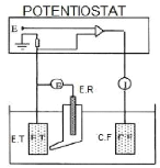
Fig.4.20 Diagram of the electrochemical cell
The potential measurement is carried out in a given aggressive
medium at a given temperature by means of a potentiostat to which are connected
three electrodes.
? The working electrode E.T constituted by the metal
studied,
?
· The reference electrode E.R which serves as a
reference for the dissolution potential, ?
· The counter electrode
C.E, which is a platinum electrode used to drain the major part
of the current flowing through the circuit when the working
electrode is subjected to an
overvoltage.
4.9.3. Diagram E=f (log/i): EVANS Diagram
Fig.4.21: a polarization curve modal
To measure the corrosion current density, the representation E
= f (i) is modified, we switch
coordinates to E = f (log / i) or EVANS
diagram in order to linearizes the polarization curve and
Chapter 4: Experimental Process
makes it possible to determine Experimentally the value of
corrosion current density icorr. THE CURRENT is obtained by
extrapolating the linear parts of the anodic and cathodic polarization curves.
This point of assistance, in cases where it is quite clear, gives access to the
characteristics of corrosion (corrosion potential and the corrosion current
density), these two linear parts, respectively called the anodic and cathodic
Tafel branches.
We see clearly on this diagram the Tafel domain in which the
potential varies linearly with the logarithm of the intensity according to the
equations of Tafel
For the anodic process:
i
(4.9)
i0(Fe)
i
(4.10)
i0(H2/Fe)
E = EFe + ba log For the cathodic process:
E = EH + bC log
70
EFe,i0(Fe),EH, i0(H2/Fe) are respectively The
equilibrium potentials and the exchange current of the couples Fe2+/Fe et H+/H2
; ba et bc Are the Tafel constants of oxidation and
reduction, (ba>0)
This graphic construction therefore provides access to these two
important corrosion data. The calculation of Tafel's equations is based on
equality:
i i
Ecorr = EFe + ba log i0(Fe)= EH + bC log
i0(H2/Fe) (4.11)
Chapter 5
Analysis of the results
Chapter 5: Analysis of the results
72
5.1. Analysis of XRD results
- Stainless steel bars:
The phases of the thin film were evaluated by the XRD analysis,
and the results are shown in the figure 5.1.
We can see that the deposited layer is an amorphous layer which
does not have a crystallographic alignment with a random orientation of the
grains, so it is inaccessible by X-ray diffraction.
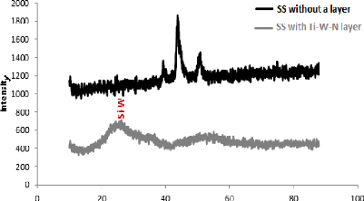
Fig.5.1: XRD spectra of the Stainless steel bars with and
without a layer of Ti-W-N
According to fig. 5.1, a bump can be observed on the angular
value 2è = 23.5°, which corresponds to tungsten silicon (Si-W) in
its amorphous form, which is requiring a subsequent heat treatment to obtain
the crystal structure of layer.
Chapter 5: Analysis of the results
2000
Fe y
vierge
SS without a layer
ss evapo Al-Si+ Ti-W-SS with double layer
1800
1600
1400
1200
1000
800
600
400
200
0
Intensity
Si-W
Fe y
Fe á
73
0 20 40 60 80 100
2-théta-scale
Fig.5.2: XRD spectra of the Stainless steel bars with and
without double layers of Al-Si and Ti-W-N
In the XRD spectra of fig.5.2, we can see again the bump
correspond to the silicon of tungsten (Si-W) at 2è = 23.5
°, we notices also iron peaks belonging to the substrate
which are iron á in 46 ° and iron y at 44
°, which means that the covering of the surface is not perfect and the
formation of an amorphous layer.
SS withTi-WN Ti
-W-N layer
ss evapo AlSi+ TiWN
SS with Al-Si and Ti-W-N double
layers
700
600
500
400
300
200
100
0
Intensity
800
0 10 20 30 40 50 60 70 80 90 100
2-théta-scale
Fig.5.3: XRD spectra of the Stainless steel bars with double
layers of Al-Si and Ti-W-N and with a layer of Ti-W-N
74
Chapter 5: Analysis of the results
Figure 5.3 shows that the intermediate layer deposited by
evaporation between the substrate and the Ti-W-N layer influences in the layer
diffraction properties in a manner which permits the appearance of peaks
corresponding to the substrate.
- Aluminum bars:
The diffraction spectra of Ti-W-N layer are shown in figure
5.4.
700
l-i vierge
Al-Si without a layer
Ti-W-N
Al-Si with a Ti-W-N layer
600
500
400
300
200
100
0
Intensity
0 10 20 30 40 50 60 70 80 90 100
2-théta-scale
Fig.5.4: XRD spectra of Aluminum-Silicon bars with and
without a layer of Ti-W-N
The spectra obtained by the XRD analysis of the Ti-W-N layer
on the aluminum substrate shows that a layer with peaks similar to that of the
substrate with an amorphous structure was formed.
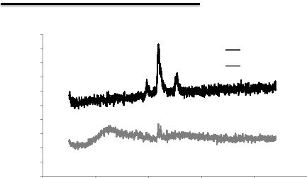
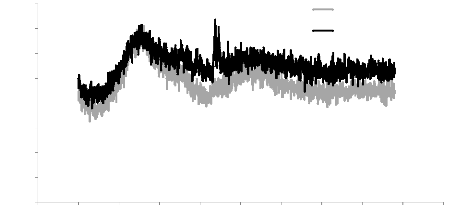
5.2. Analysis of RAMAN results
The results obtained by the RAMAN on the Ti-W-N layer for
different substrates are given by the following curves:
Chapter 5: Analysis of the results
Fig.5.5: RAMAN specter of Al-Si bar with Ti-W-N layer
Fig.5.6: RAMAN specter of stainless steel bar with Ti-W-N
layer
75
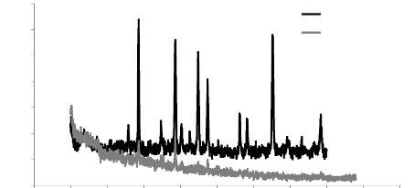
76
Chapter 5: Analysis of the results
Fig.5.7: RAMAN specter of stainless steel bar with double
layers of Al-Si and Ti-W-N
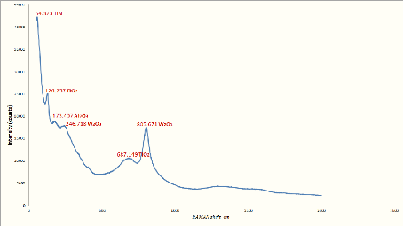
It is good to notice that the spectrum obtained for different
bars are almost the same, which means that the same elements have been observed
in the deposited layer for different substrates.
We can identify the spectrums peaks as the following:
- Peaks with the wavenumber 125 ????-1 and
675 ????-1 can be corresponded to titanium dioxide
????02 peaks [IOP/http];
- Peak with a wavenumber close to 62.5
????-1 can be corresponded to a titanium nitride ??????
peak [CHE94];
- Peak with a wavenumber close to 807
?`??-1 can be corresponded to a tungsten oxide
W203 peak [COU64];
- Peak with a wavenumber close to 172 172
????-1 observed in the spectra of stainless steel with
double layers of Al-Si and Ti-W-N can be corresponded to an aluminum oxide
????203 peak [AND02].
From the RAMAN spectrum results, it can be said that our layer
contains titanium Ti, tungsten W and nitrogen N, in the form of tungsten oxide,
titanium nitride and titanium dioxide. All of these peaks (except the
????02 peak in stainless steel substrate) are observed in different
bars.
In the contrary of the XRD results in which amorphous results
are obtained, the RAMAN results are identified all the elements of the thin
layer, which can be explained by the operating principle of each instrument.
The XRD gives results for a crystallographic analysis, so it allows us
essentially to determine the crystalline composition of the layer, which is
practically difficult without a recrystallization of the deposition by an
appropriate heat treatment.
77
Chapter 5: Analysis of the results
RAMAN, on the other hand, is used for chemical analysis. It
allows us directly to observe the chemical composition by the diffusion of the
light at the frequency of the radiation caused by the vibrations of the
molecules.
5.3. Morphological analysis
Figure 5.8 shows pictures from the Scanning Electron
Microscopy of a stainless steel bar with the double thin layer of Al-Si and
Ti-W-N.
In the picture b) we observe the formation of a layer made up
with a small nanoparticle of the order of 50 nm in diameter, and particles of
large diameter which can reach 500 nm incorporated in the surface, the
interaction of these particles creates a form of deposition called the
clusters, those clusters collide one another in order to increase their number
and size until the coalescence density where the agglomeration commences, and
the uncoated substrate surface reduces.
a) b)
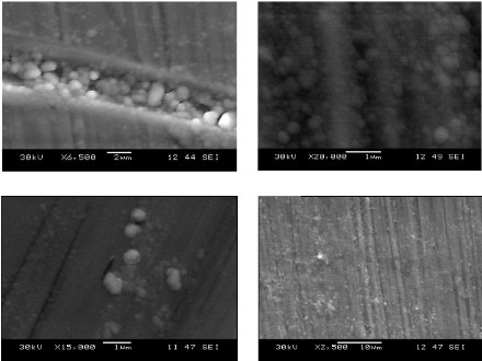
c) d)
Fig.5.8: SEM pictures, magnification of the double layers
Al-Si and Ti-W-N on stainless steel with apparition of
nanoparticles
78
Chapter 5: Analysis of the results
The morphology and the topography of the layer were studied by
the SEM on a cross section of a silicon bar with the thin layer (fig.5.9). The
cross section of the bar shows a columnar structure terminating with domes at
the surface, with grain diameter between 50 and 400 nm.
The mean thickness measured is about 1.1 rim, which lasted one
hour of deposition, what means that the growth rate is equal to 0.30 nm/ s.
That rate is a very large, which means that the deposition is not an atom by
atom layer. It is reasonable to assume that non-uniform nucleation at the
substrate surface at the beginning of deposition is the main cause of the
nonuniform growth of the layer, which cause to the random Nano-crystallization,
and this can explain the XRD results.
a) b)
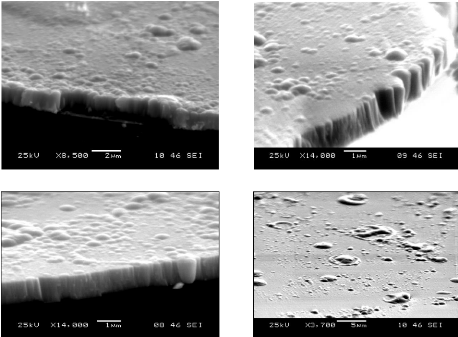
c)
d)
Fig.5.9: SEM pictures; cross section of a silicon bar with
a Ti-W-N layer
5.4. Interpretation of nanoindentation
results
The charge-discharge curves of different bars for different
depths and effort are given in the
annex, the mechanical properties obtained for each test are
given in the following curves, besides the tables of the results are given in
the Annex II.
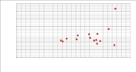
Chapter 5: Analysis of the results
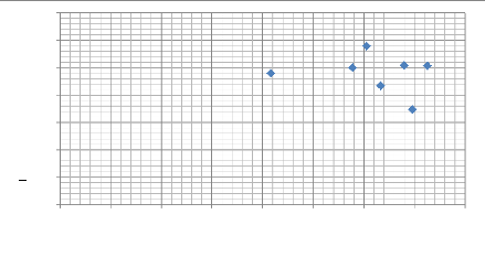
Modulus of elasticity E (G Pa )
140
120
100
40
80
60
20
0
0 50 100 150 200 250 300 350 400
Max depth (nm)
79
Fig.5.10: Scatter plot of modulus of elasticity as a
function of the max depth (nm)
Hardness (GPa)
3000
2500
2000
1500
1000
500
0
0 50 100 150 200 250 300 350 400
max depth (nm)
Fig.5.11: Scatter plot of hardness as a function of the max
depth (nm)
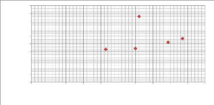
Chapter 5: Analysis of the results
Modulus of elasticity E (G Pa)
4000
8000
7000
6000
5000
3000
2000
1000
0
0 50 100 150 200 250
max depth (nm)
80
Fig.5.12: Scatter plot of modulus of elasticity as a
function of the max depth (nm)
Hardness H (MPa)
350
300
250
200
150
100
50
0
0 50 100 150 200 250
max depth (nm)
Fig.5.13 Scatter plot of hardness as a function of the max
depth (nm)
Chapter 5: Analysis of the results
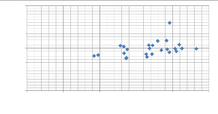
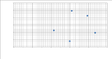
Modulus of elasticity E (GPa)
300
250
200
150
100
50
0
0 50 100 150 200 250
max depth (nm)
81
Fig.5.14 scatter plot of modulus of elasticity as a
function of the max depth (nm)
Hardness H ( M Pa)
4000
9000
8000
7000
6000
5000
3000
2000
1000
0
0 50 100 150 200 250
max depth (nm)
Fig.5.15 scatter plot of hardness as a function of the max
depth (nm)
There are in fact four factors to optimize in order to
increase the hardness of a layer: the nature of the material of deposition; its
microstructure and its architect which are more or less interdependent, and
also there is the ionic bombardment during the growth of the film.
If we make a comparison between The hardness values obtained
and the hardness values of layers with titanium, we find that our values are of
low hardness, this can be explained by the low content of interstitial element
(nitrogen) which is 5%, what means a large percentage of
82
Chapter 5: Analysis of the results
substitutional elements (the transition elements of titanium
and tungsten). Indeed, when the content of transition elements increase, the
average size of the crystallites decreases [TAK08/A], the decrease in the size
of the crystallites is the origin of the decrease in the hardness. This effect
is found in the Hall and Petch law, which reflects the fact that the tensile
stress of material is inversely proportional to the square root of the mean
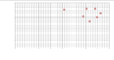
crystallite size [TAK08/A].
Modulus of elasticity E (G Pa )
170
165
160
155
150
145
140
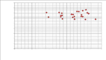
0 20 40 60 80 100 120 140 160 180 200
max depth (nm)
Fig.5.16: Scatter plot of modulus of elasticity as a
function of the max depth (nm)
Hardness H (MPa)
20000
18000
16000
14000
12000
10000
4000
8000
6000
2000
0
0 20 40 60 80 100 120 140 160 180 200
max depth (nm)
Fig.5.17: Scatter plot of hardness as a function of the max
depth (nm)
We can see in this latter bar, that its hardness is very high
compared to that measured in the preceding bars and reach a value of 17172 MPa.
Indeed, large harnesses are measured in the
83
Chapter 5: Analysis of the results
case of multilayers, and the cause of this phenomenon is
generally attributed to a combined effect including the blocking of the
dislocations at the interfaces between the layers and the intrinsic structural
differences in each layer [CIE99].
5.5. Interpretation of tribometer results 5.5.1. The
coefficient of friction
The coefficient of friction is not an intrinsic property
for a single material, but it is a value which depends on a couple of
materials. In our study, the antagonist material of our bars is the
aluminaAl2O3. The conditions of the study are given
in the previous chapter.
Figure 5.18 shows the coefficient of friction variation
for the Al-Si bare in terms of distance traveled, and Table 5.5 shows the
statistical results of the coefficient of friction obtained.
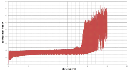
Fig.5.18: Curve of the coefficient of friction
variation for the Al-Si bare as a function of distance
traveled
|
u min
|
u max
|
u moyen
|
Standard deviation
|
|
0,00753824645653367
|
0,845997452735901
|
0,233906209468842
|
0,138767600059509
|
Table5.1 statistical results of the coefficient of
friction obtained
According to the curve, it can be seen that, from 0 m
to 7.4 m, the coefficient of friction value is low (between 0.06 and 0.26),
after that it increases abruptly to reach higher values (between 0.62 and
0.85), this is due to the existence of an aluminum oxide (alumina) layer on the
substrate surface with very low thicknesses, and which has a low coefficient of
friction. If the values corresponding to the alumina are eliminated, the
following results are obtained:
84
Chapter 5: Analysis of the results
Fig.5.19: Curve of the coefficient of friction variation
for the Al-Si bar as a function of distance traveled
without the alumina
values
|
u min
|
u max
|
u moyen
|
Standard deviation
|
|
0,1744
|
0,846
|
0,5253
|
0,1154
|
Table5.2 statistical results of the coefficient of friction
obtained
The curve in Figure 5.20 shows the friction coefficient
variation for the Al-Si bar with the Ti-W-N layer, and Table 5.7 gives the
statistical results obtained.
Fig.5.20: Curve of the coefficient of friction variation for
the Al-Si bar with Ti-W-N layer as a function of distance
traveled
85
Chapter 5: Analysis of the results
|
u min
|
u max
|
u moyen
|
Standard deviation
|
|
-0,0074
|
0,1644
|
0,0857
|
0,0145
|
Table5.3: Statistical results of the coefficient of friction
obtained
Comparing the results obtained for a piston without
and a piston with a thin layer of Ti-W-N, we noticed that the coefficient of
friction decreases from 0.5253 to 0.0857, that is to say the use of this thin
layer Allows us to reduce piston friction (if we consider that the antagonist
material is alumina) by about 613%.
By way of comparison of the coefficient of friction of
the layer for different substrates, we can give the results obtained from this
layer deposited on the stainless steel 304 and on a layer of Al-Si deposited by
evaporation on the stainless steel 304.
Fig.5.21: Curve of the coefficient of friction variation for
the stainless steel bar with Ti-W-N layer as a function of
distance traveled
|
u min
|
u max
|
u moyen
|
Standard deviation
|
|
0,0031
|
0,2477
|
0,0839
|
0,0182
|
Table5.4: Statistical results of the coefficient of
friction obtained
86
Chapter 5: Analysis of the results
Fig.5.22: Curve of the coefficient of friction variation for
the stainless steel bar with double layers of Al-Si and Ti-W-N as a function of
distance traveled
|
u min
|
u max
|
u moyen
|
Standard deviation
|
|
0,0031
|
0,2477
|
0,0839
|
0,0182
|
Table5.5: Statistical results of the coefficient of
friction obtained
From these results it can be estimated that the mean
value of the coefficient of friction for the torque Ti-W-N / Al2O3 is 0.08,
which represents in fact a low value.
If we compare the results obtained between the bar
with and a without the thin layer of Ti-W-N in terms of dissipated energy in
the contact during the work, using the Coulomb's law:
Es= u
· Fn
·Ds
u represent the sliding friction coefficient
which has a value of 0.52 for the Al-Si bar without Ti-W-N layer and 0.08 for
the Al-Si bar with Ti-W-N layer;
Fn is the normal load applied on
the contact and has a value of 1 N;
Ds is the distance traveled
between the torque and it's equal to 10 m.
The dissipated energy in the torque Al-Si/Al2O3 is
equal to 5.2 Joules for every 10 meters of piston movement i.e. 0.52 J/m, but
in the torque Ti-W-N/Al2O3 it's equal to 0.8 joules for each 10 meters that is
to say 0.08 J/m.
It should be noted that the most of this dissipated
energy in the torque (more than 95%) [COU64] is a heat energy, which requires
for the piston without layer more expense in lubrication and cooling. The
reduction of these losses results a gain in the output and therefore in the
size and mass of the cooling systems and so of the engine.
87
Chapter 5: Analysis of the results
We can add that the propagation of this heat inside the piston
under the effect of the thermal conduction causes the initiation of the
cracking and the creation of thermal stress inside the piston.
The reduction of the friction coefficient by about 613% can be
explained by the studies done by BUCKLEY [BUC67] and COURTEL [COU64] which
point that the friction is minimal on the crystalline planes with the maximum
atomic density, and on these planes in the directions of maximum atomic
density.
If we make a comparison of the friction factors in different
atomic structures we can notice that the crystalline materials with a hexagonal
structure have generally lower values of the coefficient of fiction than those
in cubic structures.
The origin of this phenomenon is that the atoms of the
hexagonal structures are strongly bound with all their neighbors and have just
some freedom to establish interfacial bonds with the atoms of the antagonistic
materials. On the other hand, the coefficient of friction depends on the force
required to break the interfacial binding between the torque surfaces
[GRA08].
The structure of aluminum is a face-centered cubic structure,
but Titan and nitrogen have a hexagonal structure, and tungsten has a centered
cubic structure, that structure has sliding planes less than those of
face-centered cubic structure.
5.5.2. Wear Rate
The method allows us to obtain the wear rate was given in
chapter 4. This method based on the measurement of the wear track using the
optical microscope. The representation of the wear track for the different bars
is given in the following figures, and the values of volume of tearing mater
and that of wear rates are given in Table 5.6.
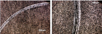
Fig.5.23 the wear track on the Al-Si bar without
layer
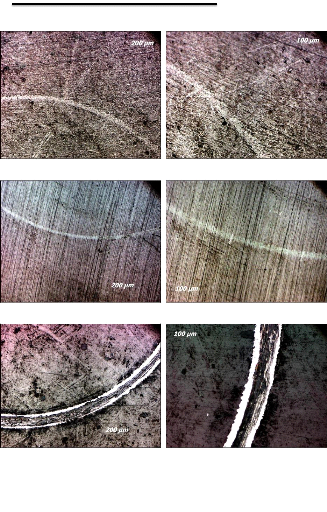
88
Chapter 5: Analysis of the results
Fig.5.24 The wear track on the Al-Si bar with the layer of
Ti-W-N
Fig.5.25 The wear track on the stainless steel bar with the
layer of Ti-W-N
Fig.5.26 The wear track on the stainless steel bar with
double layers of Al-Si and Ti-W-N
89
Chapter 5: Analysis of the results
|
Al-Si without layer
|
Al-Si with Ii-W-N
|
|
volume of tearing
mater (mm3)
|
Wear rate (mm2/N)
|
volume of tearing
mater (mm3)
|
Wear rate (mm2/N)
|
|
2325.52
|
0.2326
|
1309.18
|
0.1309
|
|
Stainless steel with Ii-W-N
|
Stainless steel with Al-Si and Ii-W-N
|
|
volume of tearing
mater (mm3)
|
Wear rate (mm2/N)
|
volume of tearing
mater (mm3)
|
Wear rate (mm2/N)
|
|
798.79
|
0.08
|
3614.29
|
0.3614
|
Table 5.6 Volume of tearing mater and the wear rate of
different bars
We can see from these results that the wear rate for a piston
without a layer has an acceptable value of 0.2326 mm2 / N, but it can be
reduced by almost the half when we add the Ti-W-N layer.
For the Ti-W-N layer, the wear rate value is varied between
0.08 and 0.13, which represents very good results for a torque of metal / metal
which has an average of values between 1 to 0.1 mm2/N [HOL58].
5.6. Corrosion test results
In this test, we search to resolve the question of whether the
thin layer of Ti-W-N is able to protect the metal substrate against corrosion
in a solution of 5% NaCl at 25° C.
The results presented in this paragraph concern the thin layer
of Ti-W-N produced by the cathode sputtering process which is shown in the
EVANS diagrams in order to obtain the corrosion rate of the layer.
The polarizability curve log(i) = f(i) allow us to determine
the corrosion potential E(I = 0) using the Tafel lines and also the corrosion
current. This quantity has a huge importance to evaluate the corrosion rate by
the Faraday law.
We can notice that the two curves are parallel, which indicate
that the two bars have an identical corrosion mechanism.
Nevertheless those results are totally in contradiction with
the fact that the different compounds formed in the layer (TiN, TiO2, W2O3...)
have good corrosion resistance characteristics in aggressive medium. We can
explicate this contradiction by saying that this layer is deposited in the form
of column with significant porosity between the grains formed, and this will
cause to concentrate the phenomenon of corrosion on small zones, that type of
corrosion called pitting (see chapter 2), which acceleration the degradation of
the layer .
These results can be overcome by:
? Variation of the layer deposition parameters, the increasing
of the deposition energy lead to more compact and denser structure;
Chapter 5: Analysis of the results
? Variation of nitrogen concentration.
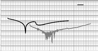
SS + TI-W-
N
1
0,1
0,01
log(i), i en A
0,001
0,0001
,00001
0,000001
0,0000001
1E-08
1E-09
1E-10
90
-0,4 -0,3 -0,2 -0,1 0 0,1 0,2 0,3 0,4
Potential (V)
Fig.5.31: Curve of polarizability of the bars of the
stainless steel with and without the layer on a logarithmic scale
Chapter 6
Piston's loads study
92
Chapter 6: Piston's loads study
6.1. Mechanical analysis of the internal combustion
engine piston using SOLIDWORKS
The piston is one of the most important components of the
internal combustion engine. Piston fails mainly due to mechanical stresses and
thermal stresses. In this paper is determined by using the finite element
method, stress and, deformation and displacement distribution.
6.1.1. Initial data
The study considers a flat sample of aluminium - silicon alloy
with dimension of (20X20 mm), subjected to 50 KN of normal force which is
equivalent to 100 bar.
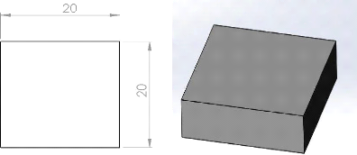
Fig.6.1. Dimensions of the piston (a) and 3D model of the
piston (b)
The material used for the piston is aluminium -silicon
eutectic alloy. The properties used are in table 1.
properties of the material value
Density 2670 kg/m3
Young's modulus 95.88 Gpa
Poisson `s ratio 0,33
Tensile yield strength 66.13 Mpa
Table 6.1.properties of the sample
93
Chapter 6: Piston's loads study
The material properties used for the Ti-W-N thin layer, are in
table 2.
properties of the material value
Density 4810 kg/m3
Young's modulus 122.73 Gpa
Poisson `s ratio 0,33
Tensile yield strength 160.8 Mpa
Table 6.2 Properties of the Ti-W-N thin layer
6.1.2. Finite element analysis of the sample 6.1.2.1.
Sample with thin coating
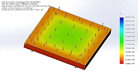
Fig.6.3. shear stress due to mechanical load for the sample
with the thin film coating
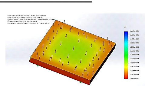
Chapter 6: Piston's loads study
94
Fig.6.4. VON MISES stress due to mechanical load for the
sample with the thin film coating
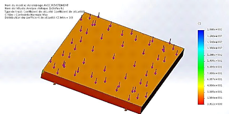
Fig.6.5. Normal stress due to mechanical load for the
sample with the thin film coating
95
Chapter 6: Piston's loads study
6.1.2.2. Sample with thin coating
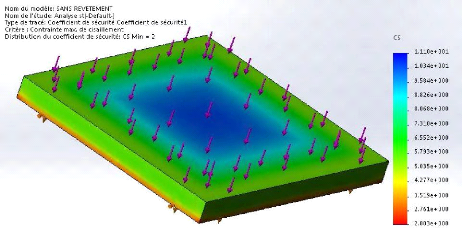
Fig.6.6. Shear stress due to mechanical load for the bare
sample
Fig.6.7. VON MISES stress due to mechanical load for the bare
sample
Chapter 6: Piston's loads study
96
Fig.6.8: Normal stress due to mechanical load for the bare
sample
|
Sample without coating
|
Sample with coating
|
|
Shear stress
|
Sc = 2
|
Sc =4.9
|
|
VON MISES stress
|
Sc = 2.2
|
Sc = 5.4
|
|
Normal stress
|
Sc = 1.6
|
Sc = 3.9
|
Table.6.3. table summarizing the minimum values of safety
coefficient 6.1.3. Analysis of the result
Table 6.3 shows clearly the impact of the thin films to the
resistance characteristic of the sample, just by using a 1um of hard thin films
the minimum value of safety coefficient jumped with 2.5 times to a much safer
zone
Analysing the figures 6.4 and 6.8 we noticed a small drop on
the VON MISES stress in the sample with the thin coating, even if this result
is not what we hoped for, but it proof that a thin film can provide much
greater characteristic just by using a small amounts of materials.
|